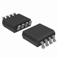
74LVC2G126DC,125 NXP Semiconductors, 74LVC2G126DC,125 Datasheet - Page 8

74LVC2G126DC,125
Manufacturer Part Number
74LVC2G126DC,125
Description
IC BUS BUFF DVR TRI-ST DL 8VSSOP
Manufacturer
NXP Semiconductors
Series
74LVCr
Datasheet
1.74LVC2G126DC125.pdf
(22 pages)
Specifications of 74LVC2G126DC,125
Package / Case
US8, 8-VSSOP
Logic Type
Buffer/Line Driver, Non-Inverting
Number Of Elements
2
Number Of Bits Per Element
1
Current - Output High, Low
32mA, 32mA
Voltage - Supply
2 V ~ 5.5 V
Operating Temperature
-40°C ~ 125°C
Mounting Type
Surface Mount
Logic Family
LVC
Number Of Channels Per Chip
2
Polarity
Non-Inverting
Supply Voltage (max)
5.5 V
Supply Voltage (min)
1.65 V
Maximum Operating Temperature
+ 125 C
Mounting Style
SMD/SMT
High Level Output Current
- 32 mA
Input Bias Current (max)
40 uA
Low Level Output Current
32 mA
Maximum Power Dissipation
300 mW
Minimum Operating Temperature
- 40 C
Output Current
50 mA
Output Type
3-State
Output Voltage
6.5 V
Propagation Delay Time
2.8 ns (Typ) @ 2.7 V or 2.4 ns (Typ) @ 3.3 V or 1.9 ns (Typ) @ 5 V
Number Of Lines (input / Output)
2 / 2
Lead Free Status / RoHS Status
Lead free / RoHS Compliant
Lead Free Status / RoHS Status
Lead free / RoHS Compliant, Lead free / RoHS Compliant
Other names
74LVC2G126DC-G
74LVC2G126DC-G
935274583125
74LVC2G126DC-G
935274583125
Available stocks
Company
Part Number
Manufacturer
Quantity
Price
Company:
Part Number:
74LVC2G126DC,125
Manufacturer:
NXP Semiconductors
Quantity:
2 900
NXP Semiconductors
11. Dynamic characteristics
Table 8.
Voltages are referenced to GND (ground = 0 V); for test circuit see
[1]
[2]
[3]
[4]
[5]
74LVC2G126
Product data sheet
Symbol Parameter
t
t
t
C
pd
en
dis
PD
Typical values are measured at T
t
t
t
C
P
f
f
C
V
N = number of inputs switching;
Σ(C
pd
en
dis
i
o
D
CC
PD
= input frequency in MHz;
L
= output frequency in MHz;
is the same as t
is the same as t
= output load capacitance in pF;
= C
is the same as t
L
is used to determine the dynamic power dissipation (P
= supply voltage in V;
× V
propagation delay nA to nY; see
enable time
disable time
power dissipation
capacitance
PD
Dynamic characteristics
CC
× V
2
× f
CC
o
2
) = sum of outputs.
× f
PLH
PZH
PLZ
i
× N + Σ(C
and t
and t
and t
PHL
PZL
PHZ
Conditions
nOE to nY; see
nOE to nY; see
per buffer; V
L
V
V
V
V
V
V
V
V
V
V
V
V
V
V
V
output enabled
output disabled
× V
amb
CC
CC
CC
CC
CC
CC
CC
CC
CC
CC
CC
CC
CC
CC
CC
CC
= 1.65 V to 1.95 V
= 2.3 V to 2.7 V
= 2.7 V
= 3.0 V to 3.6 V
= 4.5 V to 5.5 V
= 1.65 V to 1.95 V
= 2.3 V to 2.7 V
= 2.7 V
= 3.0 V to 3.6 V
= 4.5 V to 5.5 V
= 1.65 V to 1.95 V
= 2.3 V to 2.7 V
= 2.7 V
= 3.0 V to 3.6 V
= 4.5 V to 5.5 V
= 25 °C and V
2
× f
o
All information provided in this document is subject to legal disclaimers.
) where:
I
= GND to V
Figure 7
Figure 8
Figure 8
Rev. 9 — 13 September 2010
CC
= 1.8 V, 2.5 V, 2.7 V, 3.3 V and 5.0 V respectively.
CC
D
in μW).
[2]
[3]
[4]
[5]
Figure
Min
1.0
0.5
1.0
0.5
0.5
1.0
1.0
1.0
1.0
0.5
1.0
0.5
1.5
1.0
0.5
-
-
−40 °C to +85 °C
9.
Typ
3.9
2.6
2.8
2.4
1.9
4.1
2.6
2.8
2.4
1.8
3.3
1.9
3.0
2.5
1.8
17
5
[1]
Dual bus buffer/line driver; 3-state
Max
10.0
12.6
9.8
4.9
4.7
4.3
3.2
5.0
4.7
4.1
3.1
5.7
4.8
4.4
3.3
-
-
74LVC2G126
−40 °C to +125 °C
Min
1.0
0.5
1.0
0.5
0.5
1.0
1.0
1.0
1.0
0.5
1.0
0.5
1.5
1.0
0.5
-
-
© NXP B.V. 2010. All rights reserved.
Max
12.3
12.5
15.4
6.3
5.9
5.4
4.0
6.3
5.9
5.1
3.9
7.5
6.2
5.7
4.4
-
-
Unit
ns
ns
ns
ns
ns
ns
ns
ns
ns
ns
ns
ns
ns
ns
ns
pF
pF
8 of 22


