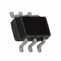
NC7WV07P6X Fairchild Semiconductor, NC7WV07P6X Datasheet - Page 3

NC7WV07P6X
Manufacturer Part Number
NC7WV07P6X
Description
IC BUFF DL ULP-A O/DRAIN SC706
Manufacturer
Fairchild Semiconductor
Series
7WVr
Specifications of NC7WV07P6X
Logic Type
Buffer/Line Driver, Non-Inverting with Open Drain
Number Of Elements
2
Number Of Bits Per Element
1
Voltage - Supply
0.9 V ~ 3.6 V
Operating Temperature
-40°C ~ 85°C
Mounting Type
Surface Mount
Package / Case
SC-70-6, SC-88, SOT-363
Logic Family
NC7WV
Number Of Channels Per Chip
Dual
Polarity
Non-Inverting
Supply Voltage (max)
3.6 V
Supply Voltage (min)
0.9 V
Maximum Operating Temperature
85 C
Mounting Style
SMD/SMT
High Level Output Current
- 24 mA
Input Bias Current (max)
0.9 uA
Low Level Output Current
24 mA
Minimum Operating Temperature
- 40 C
Number Of Lines (input / Output)
3
Output Type
Open Drain
Propagation Delay Time
6 ns at 1.65 V to 1.95 V, 3.6 ns at 2.3 V to 2.7 V, 3.3 ns at 2.7 V to 3.6 V
Logic Device Type
Buffer, Non Inverting
Supply Voltage Range
0.9V To 3.6V
Logic Case Style
SC-70
No. Of Pins
6
Operating Temperature Range
-40°C To +85°C
Filter Terminals
SMD
Rohs Compliant
Yes
Lead Free Status / RoHS Status
Lead free / RoHS Compliant
Current - Output High, Low
-
Lead Free Status / Rohs Status
Lead free / RoHS Compliant
Available stocks
Company
Part Number
Manufacturer
Quantity
Price
Part Number:
NC7WV07P6X
Manufacturer:
FAIRCHILD/仙童
Quantity:
20 000
NC7WV07 Rev. 1.0.0
Absolute Maximum Ratings
The “Absolute Maximum Ratings” are those values beyond which the safety of the device cannot be guaranteed.
The device should not be operated at these limits. The parametric values defined in the Electrical Characteristics tables
are not guaranteed at the absolute maximum ratings. The “Recommended Operating Conditions” table will define the
conditions for actual device operation.
Recommended Operating Conditions
Notes:
1. I
2. Unused inputs must be held HIGH or LOW. They may not float.
V
V
V
I
I
I
I
T
V
V
V
I
T
∆t / ∆V
IK
OK
OH
CC
OH
A
STG
CC
IN
OUT
CC
IN
OUT
Symbol
O
/I
/I
Symbol
or Ground
OL
OL
Absolute Maximum Rating must be observed.
Supply Voltage
Input Voltage
Output Voltage
Output Current in I
Free Air Operating Temperature
Minimum Input Edge Rate @ V
V
HIGH or LOW State
V
V
V
V
V
V
Supply Voltage
DC Input Voltage
DC Output Voltage
DC Input Diode Current @ V
DC Output Diode Current
DC Output Source/Sink Current
DC V
Storage Temperature Range
CC
CC
CC
CC
CC
CC
CC
HIGH or LOW State
V
V
V
= 0.0V
= 3.0V to 3.6V
= 2.3V to 2.7V
= 1.65V to 1.95V
= 1.4V to 1.6V
= 1.1V to 1.3V
= 0.9V
OUT
OUT
CC
CC
= 0V
< 0V
> V
or Ground Current per Supply Pin
CC
OH
/I
OL
(1)
IN
Parameter
IN
Parameter
= 0.8V to 2.0V, V
< 0V
(2)
3
CC
= 3.0V
− 0.5V to V
Rating
− 65 ° C to + 150 ° C
−40°C to +85°C
Rating
− 0.5V to + 4.6V
− 0.5V to + 4.6V
− 0.5V to + 4.6V
0.9V to 3.6V
www.fairchildsemi.com
0V to 3.6V
0V to 3.6V
0V to V
CC
±0.1mA
±24mA
±18mA
± 50mA
− 50mA
+ 50mA
± 50mA
± 50mA
10ns/V
±6mA
±4mA
±2mA
+ 0.5V
CC


