BLL6H0514LS-130 NXP Semiconductors, BLL6H0514LS-130 Datasheet
BLL6H0514LS-130
Available stocks


Related parts for BLL6H0514LS-130


BLL6H0514LS-130 Summary of contents
Page 1
... BLL6H0514L-130; BLL6H0514LS-130 LDMOS driver transistor Rev. 2 — 13 September 2010 1. Product profile 1.1 General description 130 W LDMOS transistor intended for pulsed applications in the 0.5 GHz to 1.4 GHz range. Table 1. Application information Typical RF performance case Mode of operation f (MHz) pulsed RF 960 to 1215 1200 to 1400 1.2 Features and benefits ...
Page 2
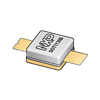
... NXP Semiconductors 2. Pinning information Table 2. Pin BLL6H0514L-130 (SOT1135A BLL6H0514LS-130 (SOT1135B [1] Connected to flange. 3. Ordering information Table 3. Type number BLL6H0514L-130 BLL6H0514LS-130 4. Limiting values Table 4. In accordance with the Absolute Maximum Rating System (IEC 60134). Symbol stg T j BLL6H0514L-130_0514LS-130 ...
Page 3
... NXP Semiconductors 5. Thermal characteristics Table 5. Symbol Z th(j-c) 6. Characteristics Table 6. Symbol Parameter V (BR)DSS V GS(th) I DSS I DSX I GSS DS(on) Table 7. Mode of operation: pulsed RF 1.2 GHz to 1.4 GHz; T test circuit. Symbol droop(pulse BLL6H0514L-130_0514LS-130 Product data sheet ...
Page 4
... NXP Semiconductors 6.1 Ruggedness in class-AB operation The BLL6H0514L-130 and BLL6H0514LS-130 are capable of withstanding a load mismatch corresponding to VSWR = through all phases under the following conditions: V Application information 7.1 Impedance information Table 8. f MHz 1200 1300 1400 Fig 1. BLL6H0514L-130_0514LS-130 Product data sheet = 50 V ...
Page 5
... NXP Semiconductors 7.2 Performance curves (dB 1. Fig 2. Power gain and drain efficiency as function of frequency; typical values ( 1.2 GHz ( 1.3 GHz ( 1.4 GHz Fig 4. Power gain as a function of load power; typical ...
Page 6
... NXP Semiconductors ( 1.2 GHz ( 1.3 GHz ( 1.4 GHz Fig 6. 8. Test information Fig 7. BLL6H0514L-130_0514LS-130 Product data sheet 160 P L (W) 120 300 s; mA Load power as a function of input power; typical values Printed-Circuit Board (PCB) material: Duroid 6006 with ...
Page 7
... NXP Semiconductors Table 9. See Figure 7 Component C1 C2, C11 C3, C4, C6, C9, C10 C5, C7, C8 C12 C13 R1 R2 [1] American Technical Ceramics type 700A or capacitor of same quality. [2] American Technical Ceramics type 100A or capacitor of same quality. [3] American Technical Ceramics type 100B or capacitor of same quality. BLL6H0514L-130_0514LS-130 Product data sheet List of components for component layout ...
Page 8
... NXP Semiconductors 9. Package outline Flanged ceramic package; 2 mounting holes; 2 leads Dimensions (1) Unit max 4.65 5.26 0.18 9.65 mm nom min 3.76 5.00 0.10 9.40 max 0.183 0.207 0.007 0.38 inches nom min 0.148 0.197 0.004 0.37 Note 1. millimeter dimensions are derived from the original inch dimensions. 2. dimension is measured 0.030 inch (0.76 mm) from the body. ...
Page 9
... NXP Semiconductors Earless flanged ceramic package; 2 leads Dimensions (1) Unit max 4.65 5.26 0.18 9.65 mm nom min 3.76 5.00 0.10 9.40 max 0.183 0.207 0.007 0.38 inches nom min 0.148 0.197 0.004 0.37 Note 1. millimeter dimensions are derived from the original inch dimensions. 2. dimension is measured 0.030 inch (0.76 mm) from the body. ...
Page 10
... NXP Semiconductors 10. Handling information CAUTION This device is sensitive to ElectroStatic Discharge (ESD). Observe precautions for handling electrostatic sensitive devices. Such precautions are described in the ANSI/ESD S20.20, IEC/ST 61340-5, JESD625-A or equivalent standards. 11. Abbreviations Table 10. Acronym LDMOS RF SMD VSWR 12. Revision history Table 11. Revision history Document ID BLL6H0514L-130_0514LS-130 v ...
Page 11
... In no event shall NXP Semiconductors be liable for any indirect, incidental, punitive, special or consequential damages (including - without limitation - lost profits, lost savings, business interruption, costs related to the removal or ...
Page 12
... Product data sheet NXP Semiconductors’ specifications such use shall be solely at customer’s own risk, and (c) customer fully indemnifies NXP Semiconductors for any liability, damages or failed product claims resulting from customer design and use of the product for automotive applications beyond NXP Semiconductors’ ...
Page 13
... NXP Semiconductors 15. Contents 1 Product profile . . . . . . . . . . . . . . . . . . . . . . . . . . 1 1.1 General description . . . . . . . . . . . . . . . . . . . . . 1 1.2 Features and benefits . . . . . . . . . . . . . . . . . . . . 1 1.3 Applications . . . . . . . . . . . . . . . . . . . . . . . . . . . 1 2 Pinning information . . . . . . . . . . . . . . . . . . . . . . 2 3 Ordering information . . . . . . . . . . . . . . . . . . . . . 2 4 Limiting values Thermal characteristics . . . . . . . . . . . . . . . . . . 3 6 Characteristics . . . . . . . . . . . . . . . . . . . . . . . . . . 3 6.1 Ruggedness in class-AB operation . . . . . . . . . 4 7 Application information 7.1 Impedance information . . . . . . . . . . . . . . . . . . . 4 7.2 Performance curves . . . . . . . . . . . . . . . . . . . . . 5 8 Test information . . . . . . . . . . . . . . . . . . . . . . . . . 6 9 Package outline . . . . . . . . . . . . . . . . . . . . . . . . . 8 10 Handling information ...