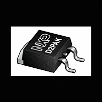
PSMN1R1-40BS NXP Semiconductors, PSMN1R1-40BS Datasheet - Page 8

PSMN1R1-40BS
Manufacturer Part Number
PSMN1R1-40BS
Description
Manufacturer
NXP Semiconductors
Datasheet
1.PSMN1R1-40BS.pdf
(14 pages)
NXP Semiconductors
PSMN1R1-40BS
Product data sheet
Fig 13. Drain-source on-state resistance as a function
Fig 15. Gate-source voltage as a function of gate
R
(m Ω )
V
(V)
GS
DSon
10
8
6
4
2
0
8
6
4
2
0
of drain current; typical values
charge; typical values
0
0
V
DS
20
40
= 8V
4.6
20V
40
80
4.8
120
60
V
GS
32V
All information provided in this document is subject to legal disclaimers.
Q
003aag670
003aaf323
I
D
(V) = 5
G
(A)
(nC)
5.2
10
20
160
Rev. 2 — 29 February 2012
80
N-channel 40 V 1.3 mΩ standard level MOSFET in D2PAK
Fig 14. Gate charge waveform definitions
Fig 16. Input, output and reverse transfer capacitances
(pF)
10
C
10
10
10
10
5
4
3
2
10
as a function of drain-source voltage; typical
values
V
-1
V
V
V
GS(pl)
DS
GS(th)
GS
Q
GS1
1
I
PSMN1R1-40BS
Q
D
GS
Q
GS2
Q
G(tot)
Q
GD
10
© NXP B.V. 2012. All rights reserved.
V
DS
003aaf324
003aaa508
C
C
C
oss
iss
rss
(V)
10
2
8 of 14


