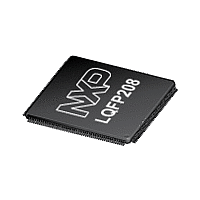
LPC2939 NXP Semiconductors, LPC2939 Datasheet - Page 19

LPC2939
Manufacturer Part Number
LPC2939
Description
The LPC2939 combine an ARM968E-S CPU core with two integrated TCM blocksoperating at frequencies of up to 125 MHz, Full-speed USB 2
Manufacturer
NXP Semiconductors
Datasheet
1.LPC2939.pdf
(99 pages)
Available stocks
Company
Part Number
Manufacturer
Quantity
Price
Company:
Part Number:
LPC2939FBD208
Manufacturer:
NXP
Quantity:
105 000
Company:
Part Number:
LPC2939FBD208,551
Manufacturer:
NXP Semiconductors
Quantity:
10 000
Company:
Part Number:
LPC2939FET208,551
Manufacturer:
NXP Semiconductors
Quantity:
10 000
NXP Semiconductors
LPC2939_3
Product data sheet
Fig 4.
AHB MULTILAYER MATRIX
AHB TO APB BRIDGES
peripheral subsystem
SYSTEM CONTROL
FLASH/SRAM/SMC
USB REGISTERS
LPC2939 overview of clock areas
EVENT ROUTER
GPIO0/1/2/3/4/5
TIMER 0/1/2/3
general subsytem
UART0/1
SPI0/1/2
GPDMA
WDT
CPU
VIC
CFID
Two of the base clocks generated by the CGU0 are used as input into a second,
dedicated CGU (CGU1). The CGU1 uses its own PLL and fractional dividers to generate
two base clocks for the USB controller and one base clock for an independent clock
output.
BASE_SYS_CLK
CGU0
branch
clocks
All information provided in this document is subject to legal disclaimers.
Rev. 03 — 7 April 2010
BA SE_ICLK0_CLK
BASE_ICLK1_CLK
BASE_IVNSS_CLK
BASE_MSCSS_CLK
BASE_PCR_CLK
ARM9 microcontroller with CAN, LIN, and USB
branch
branch
clocks
clock
branch
branch
clocks
clocks
modulation and sampling
BASE_USB_I2C_CLK
networking subsystem
CGU1
power control subsystem
control subsystem
BASE_USB_CLK
TIMER0/1 MTMR
BASE_OUT_CLK
ACCEPTANCE
RESET/CLOCK
MANAGEMENT
GENERATION
PWM0/1/2/3
GLOBAL
ADC0/1/2
CAN0/1
FILTER
LIN0/1
I2C0/1
POWER
QEI
branch
branch
branch
clock
clock
clock
LPC2939
© NXP B.V. 2010. All rights reserved.
002aae270
CLOCK
USB
OUT
19 of 99


