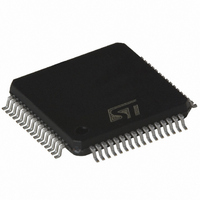
STA308A13TR STMicroelectronics, STA308A13TR Datasheet
STA308A13TR
Specifications of STA308A13TR
Available stocks


Related parts for STA308A13TR


STA308A13TR Summary of contents
Page 1
Multi-channel digital audio processor with DDX™ Features ® channels of 24-bit DDX ! >100 dB SNR and dynamic range ! Selectable 32 kHz - 192 kHz input sample rates ! 6 channels of DSD/SACD input ! Digital gain/attenuation ...
Page 2
Contents Contents 1 Block diagram . . . . . . . . . . . . . . . . . . . . . . . . . . . . . . . . . . . ...
Page 3
STA308A 7.2.7 7.2.8 7.2.9 7.2.10 7.2.11 7.2.12 7.2.13 7.2.14 7.2.15 7.2.16 7.2.17 7.2.18 7.2.19 7.2.20 7.2.21 7.2.22 7.2.23 7.2.24 7.2.25 7.2.26 7.2.27 7.2.28 7.2.29 7.2.30 7.2.31 7.2.32 7.2.33 7.2.34 7.2.35 7.2.36 7.2.37 7.2.38 7.2.39 7.2.40 7.2.41 7.2.42 7.2.43 Configuration register ...
Page 4
Contents 7.2.44 7.2.45 7.2.46 7.2.47 7.2.48 7.2.49 7.2.50 7.2.51 7.2.52 7.2.53 7.2.54 7.2.55 7.2.56 7.2.57 7.2.58 7.2.59 7.2.60 7.2.61 7.2.62 7.2.63 7.2.64 7.2.65 7.2.66 7.2.67 7.2.68 7.2.69 7.2.70 7.2.71 7.2.72 7.2.73 7.2.74 7.2.75 7.2.76 7.2.77 7.2.78 7.3 Reading a coefficient ...
Page 5
STA308A 7.5 Writing a single coefficient to RAM . . . . . . . . . . . . . . . . . . . . . . . . . . . . . 55 7.6 Writing ...
Page 6
List of tables List of tables Table 1. Device summary . . . . . . . . . . . . . . . . . . . . . . . . . . . . . . ...
Page 7
STA308A List of figures Figure 1. Block diagram . . . . . . . . . . . . . . . . . . . . . . . . . . . . . . . . ...
Page 8
Block diagram 1 Block diagram Figure 1. Block diagram LRCKI BICKI SDI12 SDI34 SDI56 SDI78 PLLB Figure 2. Channel signal flow 6 Inputs From DSD Interp_Rate 8 Inputs From I2S From Mix#1 Engine PreScale Or Previous Channel Biquad#10 Output (CxBLP) ...
Page 9
STA308A 2 Pin connections Figure 3. Pin connection (Top view) Table 2. Pin description Pin 1 5-V tolerant TTL input buffer MVO/DSD_CLK 6 5-V tolerant TTL input buffer SDI_78/DSD_6 7 5-V tolerant TTL input buffer SDI_56/DSD_5 8 5-V tolerant TTL ...
Page 10
Pin connections Table 2. Pin description (continued) Pin CMOS input buffer with 17 pull-down Bidirectional buffer: 5-V tolerant TTL schmitt trigger 18 input; 3.3-V capable 2mA slew-rate controlled output. 5-V tolerant TTL schmitt 19 trigger input buffer 5-V tolerant TTL ...
Page 11
STA308A Table 2. Pin description (continued) Pin 3.3-V capable TTL 2mA 48 output buffer 3.3-V capable TTL 2mA 49 output buffer 3.3-V capable TTL 2mA 50 output buffer 3.3-V capable TTL 4mA 51 output buffer 3.3-V capable TTL 2mA 55 ...
Page 12
Electrical specification 3 Electrical specification 3.1 Absolute maximum ratings Table 3. Absolute maximum ratings Symbol V 3.3-V I/O power supply DD V 3.3-V logic power supply DDA V Voltage on input pins i V Voltage on output pins o T ...
Page 13
STA308A 3.4 Electrical specifications The following specifications are valid for VDD = 3.3V ± 0.3V, VDDA = 3.3V ± 0.3V and Tamb = °C, unless otherwise stated Table 6. General interface electrical specifications Symbol I Low-level input ...
Page 14
Pin description 4 Pin description Master volume override (MVO) This pin enables the user to bypass the volume control on all channels. When MVO is pulled high, the master volume register is set to 0x00, which corresponds to its full ...
Page 15
STA308A bus operation The STA308A supports the I slave) and the output port SDA_OUT (slave to master). This protocol defines any device that sends data on to the bus as a transmitter and any device that ...
Page 16
I C bus operation address and if a match is found, it acknowledges the identification on SDA bus during the th 9 -bit time. The byte following the device identification byte is the internal space address. 5.3 Write operation ...
Page 17
STA308A 6 Application reference schematic Figure 6. Reference schematic for STA308A-based application OUT1_B OUT7_A 49 32 OUT1_A OUT7_B 50 31 EAPD OUT8_A 51 30 VDD3.3_6 OUT8_B 52 29 GND_6 VDD3.3_3 GND_3 54 27 BICKO 26 NC ...
Page 18
Registers 7 Registers 7.1 Register summary Table 8. Register summary Addr Name Configuration 0x00 CONFA 0x01 ConfB 0x02 ConfC 0x03 ConfD 0x04 ConfE 0x05 ConfF 0x06 ConfG 0x07 ConfH 0x08 ConfI Volume control 0x09 MMUTE 0x0A Mvol 0x0B C1Vol 0x0C ...
Page 19
STA308A Table 8. Register summary (continued) Addr Name 0x1C C34im 0x1D C56im 0x1E C78im AutoMode 0x1F Auto1 0x20 Auto2 0x21 Auto3 0x22 PreEQ 0x23 Ageq 0x24 Bgeq 0x25 Cgeq 0x26 Dgeq 0x27 Egeq Processing loop 0x28 BQlp 0x29 MXlp Processing ...
Page 20
Registers Table 8. Register summary (continued) Addr Name 0x38 C34om 0x39 C56om 0x3A C78om User-defined coefficient RAM 0x3B Cfaddr1 0x3C Cfaddr2 CFA7 0x3D B1cf1 0x3E B1cf2 0x3F B1cf3 0x40 B2cf1 0x41 B2cf2 0x42 B2cf3 0x43 A1cf1 0x44 A1cf2 0x45 A1cf3 ...
Page 21
STA308A 7.2 Register description 7.2.1 Configuration register A (0x00 COS1 COS0 1 0 Bit The DDX8000 supports sample rates of 32 kHz, 44.1 kHz, 48 kHz, 88.2 kHz, 96 kHz, 176.4 ...
Page 22
Registers I IR[ 176.4 10 192 11 DSD Bit Setting the DSPB bit bypasses the biquad function of the Omega DDX core ...
Page 23
STA308A 7.2.2 Configuration register B (0x01) - serial input formats D7 D6 Bit Serial data interface The STA308A audio serial input interfaces with standard digital audio components ...
Page 24
Registers The table below lists the serial audio input formats supported by STA308A as related to BICKI = fs, 192 kHz. BICKI 24/ where sampling rate, ...
Page 25
STA308A 7.2.3 Configuration register C (0x02) - serial output formats D7 D6 Bit The STA308A features a serial audio output interface that consists of 8 channels. The ...
Page 26
Registers 7.2.4 Configuration register D (0x03 MPC CSZ4 1 1 Bit The DDX power output mode selects how the DDX output timing is configured. Different power devices use different output modes. ...
Page 27
STA308A 7.2.5 Configuration register E (0x04 C8BO C7BO 0 0 Bit Each individual ...
Page 28
Registers In dynamic range compression mode the limiter threshold values vary with the volume settings allowing a nighttime listening mode that provides a reduction in the dynamic range regardless of the volume level. Bit setting ...
Page 29
STA308A 7.2.7 Configuration register G (0x06 MPCV DCCV 0 0 Bit Bit The STA308A features a DDX processing mode that minimizes the amount of noise generated in ...
Page 30
Registers Bit Bit 7.2.8 Configuration register H (0x07 ECLE LDTE 0 1 Bit RW RST Bit RW RST The ZCE bit enables zero-crossing volume ...
Page 31
STA308A Bit Setting the IDE bit enables this function, which looks at the input I automatically mute if the signals are perceived as invalid. Bit Detects loss of input MCLK in binary ...
Page 32
Registers 7.2.10 Master mute register (0x09 7.2.11 Master volume register (0x0A MV7 MV6 1 1 Note: Value of volume derived from MVOL is dependent on AMV AutoMode volume settings. 7.2.12 Channel 1 volume (0x0B ...
Page 33
STA308A 7.2.16 Channel 5 volume (0x0F C5V7 C5V6 0 1 7.2.17 Channel 6 volume (0x10 C6V7 C6V6 0 1 7.2.18 Channel 7 volume (0x11 C7V7 C7V6 0 1 7.2.19 Channel 8 volume (0x12) D7 ...
Page 34
Registers 7.2.23 Channel 4 volume trim, mute, bypass (0x16 C4M C4VBP 0 0 7.2.24 Channel 5 volume trim, mute, bypass (0x17 C5M C5VBP 0 0 7.2.25 Channel 6 volume trim, mute, bypass (0x18 C6M ...
Page 35
STA308A When ZCE = 0, volume updates occur immediately. Each channel also contains an individual channel volume bypass particular channel has volume bypassed via the CnVBP = 1 register then only the channel volume setting for that particular ...
Page 36
Registers 7.2.28 Channel input mapping channels 1 and 2 (0x1B C2IM2 0 7.2.29 Channel input mapping channels 3 and 4 (0x1C C4IM2 0 7.2.30 Channel input mapping channels 5 and 6 (0x1D C6IM2 1 ...
Page 37
STA308A 7.2.32 AUTO1 - AutoModes EQ, volume, GC (0x1F AMDM AMGC2 0 0 Bit RW 1 setting AMEQ to any setting other than 00 enables AutoMode EQ, biquads 1-5 are not user programmable. Any coefficient ...
Page 38
Registers 7.2.33 AUTO2 - AutoModes bass management2 (0x20 SUB RSS1 1 0 Bit Bit Setting the AMBMME bit enables the proper mixing to take place for various preset bass management ...
Page 39
STA308A FSS - front speaker size SUB - subwoofer When AMBMXE = 1, biquad #7 on channels 1-6 are utilized for bass-management crossover filter, this biquad is not user programmable in this mode. The XO settings determine the crossover frequency ...
Page 40
Registers 7.2.35 PREEQ - Preset EQ settings (0x22 XO2 XO1 1 0 000 001 010 011 100 101 110 111 00000 00001 00010 00011 00100 00101 00110 00111 01000 01001 01010 01011 01100 01101 01110 01111 10000 10001 ...
Page 41
STA308A 10100 10101 10110 10111 11000 11001 11010 11011 11100 11101 11110 11111 7.2.36 AGEQ - graphic EQ 80-Hz band (0x23 7.2.37 BGEQ - graphic EQ 300-Hz band (0x24 7.2.38 CGEQ - graphic EQ 1-kHz band ...
Page 42
Registers 7.2.40 EGEQ - graphic EQ 8-kHz band (0x27 11111 11110 11101 … 10000 01111 01110 … 00001 00000 7.2.41 Biquad internal channel loop-through (0x28 C8BLP C7BLP 0 0 Each internal processing channel can receive two ...
Page 43
STA308A 7.2.42 Mix internal channel loop-through (0x29 C8MXLP C7MXLP 0 0 Each internal processing channel can receive two possible sets of inputs at the inputs to the Mix#1 block. The inputs can come from the outputs of the ...
Page 44
Registers 7.2.45 Tone control (0x2C TTC3 TTC2 0 1 This is the tone control boost / cut as a function of BTC and TTC bits. BTC[3:0] / TTC[3:0) 0000 0001 … 0111 0110 0111 1000 1001 … 1101 ...
Page 45
STA308A 7.2.49 Limiter 1 attack/release threshold (0x30 L1AT3 L1AT2 0 1 7.2.50 Limiter 2 attack/release rate (0x31 L2A3 L2A2 0 1 7.2.51 Limiter 2 attack/release threshold (0x32 L2AT3 L2AT2 0 1 7.2.52 Bit description ...
Page 46
Registers In AC mode the attack and release thresholds are set relative to full-scale. In DRC mode the attack threshold is set relative to the maximum volume setting of the channels mapped to that limiter and the release threshold is ...
Page 47
STA308A 0000 0001 0010 0011 0100 0101 0110 0111 1000 1001 1010 1011 1100 1101 1110 1111 0000 0001 0010 0011 0100 0101 0110 0111 1000 1001 1010 1011 1100 1101 1110 1111 LnR[3:0] 0.5116 (fast) 0.1370 0.0744 0.0499 0.0360 ...
Page 48
Registers 0000 0001 0010 0011 0100 0101 0110 0111 1000 1001 1010 1011 1100 1101 1110 1111 0000 0001 0010 0011 0100 0101 0110 0111 1000 1001 1010 1011 1100 1101 1110 1111 48/63 LnRT[3:0] -∞ -29 dB -20 dB ...
Page 49
STA308A 0000 0001 0010 0011 0100 0101 0110 0111 1000 1001 1010 1011 1100 1101 1110 1111 7.2.53 Channel 1 and 2 output timing (0x33 C2OT2 1 7.2.54 Channel 3 and 4 output timing (0x34 C4OT2 ...
Page 50
Registers 7.2.56 Channel 7 and 8 output timing (0x36 C8OT2 1 The centering of the individual channel PWM output periods can be adjusted by the output timing registers. PWM slot settings can be chosen to insure that pulse ...
Page 51
STA308A 2 7.2.60 Channel I S output mapping channels 7 and 8 (0x3A C8OM2 1 2 Each I S output channel can receive data from any channel output of the volume block. Which channel a particular I register ...
Page 52
Registers 7.2.64 Coefficient b1 data register, bits 15:8 (0x3E C1B15 C1B14 0 0 7.2.65 Coefficient b1 data register, bits 7:0 (0x3F C1B7 C1B6 0 0 7.2.66 Coefficient b2 data register, bits 23:16 (0x40 C2B23 ...
Page 53
STA308A 7.2.71 Coefficient a1 data register, bits 7:0 (0x45 C3B7 C3B6 0 0 7.2.72 Coefficient a2 data register, bits 23:16 (0x46 C4B23 C4B22 0 0 7.2.73 Coefficient a2 data register, bits 15:8 (0x47 C4B15 ...
Page 54
Registers 7.2.78 Coefficient write control register (0x4C Coefficients for EQ and Bass Management are handled internally in the STA308A via RAM. Access to this RAM is available to the user via collection of I ...
Page 55
STA308A 7.5 Writing a single coefficient to RAM 1. write top 2-bits of address write bottom 8-bits of address write top 8-bits of coefficient write middle 8-bits of coefficient in I ...
Page 56
Equalization and mixing 8 Equalization and mixing Figure 8. Channel mixer 8.1 Post-scale The STA308A provides one additional multiplication after the last interpolation stage and before the distortion compensation on each channel. This is a 24-bit signed fractional multiply. The ...
Page 57
STA308A Table 9. RAM block for biquads, mixing, and bass management (continued) Index (decimal … … 99 100 … 399 400 401 402 … 407 408 409 … 415 416 417 … 423 424 425 ...
Page 58
Equalization and mixing Table 9. RAM block for biquads, mixing, and bass management (continued) Index (decimal) … 527 8.2 Variable max power correction 8.2.1 MPCC1-2 (0x4D, 0x4E) MPCC bits determine the 16 MSBs of the MPC compensation coefficient. This coefficient ...
Page 59
STA308A 8.4 PSCorrect registers ADC is used to input ripple data to SDI78. The left channel (7) is used internally. No audio data can therefore be used on these channels. Though all channel mapping and mixing from other inputs to ...
Page 60
Package information 9 Package information In order to meet environmental requirements, ST offers these devices in ECOPACK packages. These packages have a Lead-free second level interconnect. The category of second Level Interconnect is marked on the package and on the ...
Page 61
... STA308A 10 Trademarks and other acknowledgements DDX is a registered trademark of Apogee Technology Inc. ECOPACK is a registered trademark of STMicroelectronics. Trademarks and other acknowledgements 61/63 ...
Page 62
Revision history 11 Revision history Table 10. Document revision history Date May-2004 Nov-2005 June-2006 July-2007 62/63 Revision 1 Initial release. 2 Changed in page 4 value T 3 Changed in Figure 4 and Table 2 the name of the pins ...
Page 63
... STA308A Information in this document is provided solely in connection with ST products. STMicroelectronics NV and its subsidiaries (“ST”) reserve the right to make changes, corrections, modifications or improvements, to this document, and the products and services described herein at any time, without notice. All ST products are sold pursuant to ST’s terms and conditions of sale. ...