AD539JD Analog Devices Inc, AD539JD Datasheet - Page 4
AD539JD
Manufacturer Part Number
AD539JD
Description
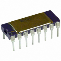
IC MULT/DIV DUAL CH LIN 16-CDIP
Manufacturer
Analog Devices Inc
Specifications of AD539JD
Rohs Status
RoHS non-compliant
Function
Analog Multiplier/Divider
Number Of Bits/stages
2
Package / Case
16-CDIP (0.300", 7.62mm)
Number Of Elements
2
Output Type
Single
Power Supply Requirement
Dual
Single Supply Voltage (typ)
Not RequiredV
Single Supply Voltage (min)
Not RequiredV
Single Supply Voltage (max)
Not RequiredV
Dual Supply Voltage (typ)
±5/±9/±12V
Dual Supply Voltage (min)
±4.5V
Dual Supply Voltage (max)
±15V
Operating Temperature Classification
Commercial
Mounting
Through Hole
Pin Count
16
Package Type
SBCDIP
Lead Free Status / RoHS Status
Not Compliant
Available stocks
Company
Part Number
Manufacturer
Quantity
Price

Part Number:
AD539JD
Manufacturer:
ADI/亚德诺
Quantity:
20 000


Parameter
CONTROL INPUT, V
CURRENT OUTPUT
VOLTAGE OUTPUTS, V
TEMPERATURE RANGE
POWER SUPPLIES
1
2
3
4
AD539
Tested on all production units at final electrical test. Results from those tests are used to calculate outgoing quality levels.
Resistance value and absolute current outputs subject to 20% tolerance.
Specification assumes the external op amp is trimmed for negligible input offset.
Includes all errors.
Nominal Full-Scale Input
Operational Range, Degraded
Input Resistance
Offset Voltage
Power Supply Sensitivity
Gain
Full-Scale Output Current
Peak Output Current
Output Offset Current
Output Offset Voltage
Output Resistance
Scaling Resistors
Multiplier Transfer Function
Total Multiplication Error
Control Feedthrough
Rated Performance
Operational Range
Current Consumption
Performance
T
Absolute Gain Error
T
Channel 1
Channel 2
Either Channel
Multiplier Scaling Voltage, V
Power Supply Sensitivity
T
T
+V
−V
MIN
MIN
MIN
MIN
Accuracy
T
S
S
MIN
to T
to T
to T
to T
to T
MAX
MAX
MAX
MAX
MAX
2
X
2
W1
AND V
3
4
W2
3
U
See Figure 20, V
Test Conditions/Comments
See Figure 20
V
V
V
V
V
V
V
Z1, W1 to CH1
Z2, W2 to CH2
See Figure 20
V
V
X
X
X
X
S
X
Y
X
X
= ±7.5 V
= 0.1 V to 3.0 V, V
= 0.1 V to 3.0 V, V
= 3 V, V
= 3.3 V, V
= 0 V, V
= 0 V
≤ 3 V, −2 V < V
= 0 V to 3 V, V
Y
Y
= ±2 V
= 0 V
Y
= ±5 V,
X
Y
Y
= 0 V,
= 0 V
< +2 V
Y
Y
= ±2 V
= ±2 V
Rev. B | Page 4 of 20
0
±4.5
Min
+3.2
±2
0.98
V
1
W
= −V
AD539J
0.04
Typ
3.0
500
1
3
30
0.2
0.3
±1
±2.8
0.2
3
1.2
6
6
1.0
0.5
1
1
2
25
30
8.5
18.5
X
× V
Y
/V
Max
4
0.4
1.5
10
U
1.02
2
2.5
60
+70
±15
10.2
22.2
1
1
1
1
1
1
1
1
1
0
±4.5
Min
+3.2
±2
0.99
V
W
1
= −V
AD539K
Typ
3.0
500
1
2
30
0.1
0.15
±1
±2.8
0.2
3
1.2
6
6
1.0
0.5
0.5
0.04
0.6
1
15
15
8.5
18.5
X
× V
Y
/V
Max
2
0.2
1.5
10
1.01
1
1.5
30
+70
±15
10.2
22.2
1
1
U
1
1
1
1
1
1
1
−55
±4.5
Min
+3.2
±2
0.98
V
W
1
= −V
AD539S
Typ
3.0
500
1
2
30
0.2
0.25
±1
±2.8
0.2
3
1.2
6
6
1.0
0.5
1.0
0.04
1
2
15
60
8.5
18.5
X
× V
Y
/V
Max
4
5
0.4
0.5
1.5
10
1.02
2
3
2.5
4
60
120
+125
±15
10.2
22.2
1
1
1
1
U
1
1
1
1
1
1
1
1
1
Unit
V
V
Ω
mV
mV
μV/V
dB
dB
mA
mA
μA
mV
kΩ
kΩ
kΩ
V
%
%
%/V
% FSR
%
mV
mV
°C
V
mA
mA
Related parts for AD539JD
Image
Part Number
Description
Manufacturer
Datasheet
Request
R

Part Number:
Description:
±1.7g Dual-Axis IMEMS Accelerometer Evaluation Board
Manufacturer:
Analog Devices Inc
Datasheet:

Part Number:
Description:
Inertial Sensor Evaluation System
Manufacturer:
Analog Devices Inc
Datasheet:
Part Number:
Description:
Manufacturer:
Analog Devices Inc
Datasheet:
Part Number:
Description:
Manufacturer:
Analog Devices Inc
Datasheet:
Part Number:
Description:
Manufacturer:
Analog Devices Inc
Datasheet:
Part Number:
Description:
Manufacturer:
Analog Devices Inc
Datasheet:
Part Number:
Description:
Manufacturer:
Analog Devices Inc
Datasheet:
Part Number:
Description:
Manufacturer:
Analog Devices Inc
Datasheet:
Part Number:
Description:
Manufacturer:
Analog Devices Inc
Datasheet:
Part Number:
Description:
Manufacturer:
Analog Devices Inc
Datasheet:
Part Number:
Description:
Manufacturer:
Analog Devices Inc
Datasheet:
Part Number:
Description:
Manufacturer:
Analog Devices Inc
Datasheet:
Part Number:
Description:
Manufacturer:
Analog Devices Inc
Datasheet: