AD539JD Analog Devices Inc, AD539JD Datasheet - Page 13
AD539JD
Manufacturer Part Number
AD539JD
Description
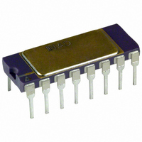
IC MULT/DIV DUAL CH LIN 16-CDIP
Manufacturer
Analog Devices Inc
Specifications of AD539JD
Rohs Status
RoHS non-compliant
Function
Analog Multiplier/Divider
Number Of Bits/stages
2
Package / Case
16-CDIP (0.300", 7.62mm)
Number Of Elements
2
Output Type
Single
Power Supply Requirement
Dual
Single Supply Voltage (typ)
Not RequiredV
Single Supply Voltage (min)
Not RequiredV
Single Supply Voltage (max)
Not RequiredV
Dual Supply Voltage (typ)
±5/±9/±12V
Dual Supply Voltage (min)
±4.5V
Dual Supply Voltage (max)
±15V
Operating Temperature Classification
Commercial
Mounting
Through Hole
Pin Count
16
Package Type
SBCDIP
Lead Free Status / RoHS Status
Not Compliant
Available stocks
Company
Part Number
Manufacturer
Quantity
Price

Part Number:
AD539JD
Manufacturer:
ADI/亚德诺
Quantity:
20 000


Table 4. Summary of Operating Conditions and
Performance for the AD539 When Used with Various
External Op Amp Output Amplifiers
Operating Conditions
Op Amp Supply Voltages
Op Amp Compensation Capacitor
Feedback Capacitor, C
−3 dB Bandwidth, V
Load Capacitance
HF Feedthrough
RMS Output Noise
1
In all cases, 0.47 μF ceramic supply decoupling capacitors were
used at each IC pin, the AD539 supplies were ±5 V, and the
control compensation capacitor C
Minimal Wideband Configurations
The maximum bandwidth can be achieved using the AD539
with simple resistive loads to convert the output currents to
voltages. These currents (nominally ±1 mA FS, ±2.25 mA peak,
into short-circuit loads) are shunted by their source resistance
of 1.25 kΩ (each channel). Calculations of load power and
effective scaling-voltage must allow for this shunting effect
when using resistive loads. The output power is quite low in this
mode, and the device behaves more like a voltage-controlled
attenuator than a classical multiplier. The matching of gain and
phase between the two channels is excellent. From dc to 10 MHz,
the gains are typically within ±0.025 dB (measured using preci-
sion 50 Ω load resistors) and the phase difference within ±0.1°.
For a given load resistance, the output power can be quadrupled
by using both channels in parallel, as shown in Figure 21. The
small signal silicon diode, D, connected between ground and
Table 5. Summary of Performance for Minimal Configuration
Load Resistance
FS Output Voltage
FS Output
Peak Output Voltage
Peak Output
Effective Scaling Voltage, V
1
2
For the circuit of Figure 20.
Peak negative voltage swing limited by output compliance.
N/A means not applicable.
V
V
V
DC
AC (RMS)
Power in Load
DC
AC (RMS)
Power in Load
X
X
X
= 1 V, BW 10 Hz to10 kHz
= −0.01 V, f = 5 MHz
= 1 V, BW 10 Hz to 5 MHz
X
= 1 V
F
U
’
C
was 3 nF.
50 Ω
±92.6 mV
65.5 mV rms
0.086 mW
−10.5 dBm
±210 mV
148 mV rms
0.44 mW
−7 dBm
67.5 V
AD711
±15 V
None
None
900 kHz
<1 nF
N/A
50 μV
120 μV
1
LH0032
±10 V
1 pF to 5 pF
1 pF to 4 pF
25 MHz
<10 pF
−70 dB
30 μV
500 μV
75 Ω
±134 mV
94.7 mV rms
0.12 mW
−9.2 dBm
±300 mV
212 mV rms
0.6 mW
−4.4 dBm
46.7 V
Rev. B | Page 13 of 20
1
100 Ω
±172 mV
122 mV rms
0.15 mW
−8.3 dBm
±388 mV
274 mV rms
0.75 mW
−2.5 dBm
36.3 V
BASE COMMON (Pin 12 and Pin 13) provides extra voltage
compliance at the output nodes in the negative direction (to
−1 V at 25°C); it is not required if the output swing does not
exceed −300 mV. Table 5 compares performance for various
load resistances, using this configuration.
Figure 9 shows the high frequency response for Figure 21 with
the AD539 in a carefully shielded 50 Ω test environment; the
test system response was first characterized and this
background removed by digital signal processing to show the
inherent circuit response.
In many applications phase linearity over frequency is important.
Figure 10 shows the deviation from an ideal linear-phase response
for a typical AD539 over the frequency range dc to 10 MHz, for
V
tial phase linearity (the stability of phase over the signal window
at a fixed frequency) is shown in Figure 11 for f = 3.579 MHz
and various values of V
V
it is recommended that a ground-referenced, negative-going
signal be used.
V
Y
X
Y
= 3 V; the peak deviation is slightly more than 1°. Differen-
above 1 V; in applications where this characteristic is critical,
V
X
0.47µF
Figure 21. Minimal Single-Channel Multiplier
C
150 Ω
±242 mV
171 mV rms
0.195 mW
−7.1 dBm
±544 mV
385 mV rms
1 mW
0 dBm
25.8 V
C
= 3nF
+V
–V
(16-Lead SBDIP and PDIP Shown)
S
S
1
2
3
4
5
6
7
8
X
V
HF COMP
V
+V
–V
V
INPUT
COMMON
OUTPUT
COMMON
. The most rapid variation occurs for
X
Y1
Y2
S
S
AD539
COMMON
433 mV rms
0.312 mW
Note
Note
600 Ω
±612 mV
−5.05 dBm
±1 mV
±1 V
10.2 V
OUTPUT
OUTPUT
BASE
CHAN1
CHAN2
1
1
W2
W1
Z2
Z1
16
15
14
13
12
10
11
9
NC
NC
NC
NC
*
D*
REQUIRED IF LOAD
RESISTANCE >300Ω
Open Circuit
±1 V
Note
N/A
N/A
±1 V
Note
±1 V
Note
5 V
2
R
1
1
1
AD539
V
L
W
=
V
V
X
V
U
Y
Related parts for AD539JD
Image
Part Number
Description
Manufacturer
Datasheet
Request
R

Part Number:
Description:
±1.7g Dual-Axis IMEMS Accelerometer Evaluation Board
Manufacturer:
Analog Devices Inc
Datasheet:

Part Number:
Description:
Inertial Sensor Evaluation System
Manufacturer:
Analog Devices Inc
Datasheet:
Part Number:
Description:
Manufacturer:
Analog Devices Inc
Datasheet:
Part Number:
Description:
Manufacturer:
Analog Devices Inc
Datasheet:
Part Number:
Description:
Manufacturer:
Analog Devices Inc
Datasheet:
Part Number:
Description:
Manufacturer:
Analog Devices Inc
Datasheet:
Part Number:
Description:
Manufacturer:
Analog Devices Inc
Datasheet:
Part Number:
Description:
Manufacturer:
Analog Devices Inc
Datasheet:
Part Number:
Description:
Manufacturer:
Analog Devices Inc
Datasheet:
Part Number:
Description:
Manufacturer:
Analog Devices Inc
Datasheet:
Part Number:
Description:
Manufacturer:
Analog Devices Inc
Datasheet:
Part Number:
Description:
Manufacturer:
Analog Devices Inc
Datasheet:
Part Number:
Description:
Manufacturer:
Analog Devices Inc
Datasheet: