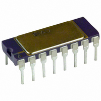
AD539JD Analog Devices Inc, AD539JD Datasheet - Page 15

AD539JD
Manufacturer Part Number
AD539JD
Description
IC MULT/DIV DUAL CH LIN 16-CDIP
Manufacturer
Analog Devices Inc
Specifications of AD539JD
Rohs Status
RoHS non-compliant
Function
Analog Multiplier/Divider
Number Of Bits/stages
2
Package / Case
16-CDIP (0.300", 7.62mm)
Number Of Elements
2
Output Type
Single
Power Supply Requirement
Dual
Single Supply Voltage (typ)
Not RequiredV
Single Supply Voltage (min)
Not RequiredV
Single Supply Voltage (max)
Not RequiredV
Dual Supply Voltage (typ)
±5/±9/±12V
Dual Supply Voltage (min)
±4.5V
Dual Supply Voltage (max)
±15V
Operating Temperature Classification
Commercial
Mounting
Through Hole
Pin Count
16
Package Type
SBCDIP
Lead Free Status / RoHS Status
Not Compliant
Available stocks
Company
Part Number
Manufacturer
Quantity
Price
Part Number:
AD539JD
Manufacturer:
ADI/亚德诺
Quantity:
20 000
A 50 MHZ VOLTAGE-CONTROLLED AMPLIFIER
Figure 24 is a circuit for a 50 MHz voltage-controlled amplifier
(VCA) suitable for use in high quality video-speed applications.
The outputs from the two signal channels of the AD539 are
applied to the op amp in a subtracting configuration. This
connection has two main advantages: first, it results in better
rejection of the control voltage, particularly when overdriven
(V
noninverting or inverting response, using either input, V
V
Therefore, the gain is unity at V
range to 3.3 V, the maximum gain in this configuration is
about 4.3 dB.
The −3 dB bandwidth of this circuit is over 50 MHz at a full
gain and is not substantially affected at lower gains. When V
Y2
X
, respectively. In this circuit, the output of the op amp equals
< 0 V or V
V
OUT
=
V
X
X
> 3.3 V). Secondly, it provides a choice of either
(
V
2
Y
1
V
−
V
Y
V
V
NOTES
1. THOMPSON-CSF BAR. 10 OR SIMILAR SCHOTTKY DIODE
SHORT DIRECT CONNECTION TO GROUND PLANE.
2
Y2
Y2
V
)
X
for
IN
IN
Figure 24. A Wide Bandwidth Voltage-Controlled Amplifier (16-Lead SBDIP and PDIP Shown)
V
X
+9V
–9V
X
= 2 V. Because V
D1
>
0
V
75Ω
10Ω
10Ω
C
600pF
C
75Ω
F
C
3000pF
X
75Ω
can over-
1µF
1µF
Y1
1
2
3
4
5
6
7
8
or
V
HF COMP
V
+V
–V
V
INPUT
COMMON
OUTPUT
COMMON
X
Y1
Y2
X
Rev. B | Page 15 of 20
S
S
is
AD539
COMMON
OUTPUT
OUTPUT
BASE
CHAN1
CHAN2
W2
W1
Z1
Z2
zero (or slightly negative, to override the residual input offset)
there is still a small amount of capacitive feedthrough at high
frequencies; therefore, extreme care is required in laying out the
PC board to minimize this effect. In addition, for small values
of V
output can cause a dip in the response where they are out of
phase. Figure 15 shows the ac response from the noninverting
input, with the response from the inverting input, V
identical. Test conditions include V
V
The feedthrough at V
With the VCA driving a 75 Ω load and the transient response of
the signal channel at V
Figure 16. The rise and fall times are approximately 7 ns.
A more detailed description of this circuit, including differential
gain and phase characteristics, is given in the
Note, Low Cost, Two Chip Voltage-Controlled Amplifier and
Video Switch, available from Analog Devices.
X
16
15
14
13
12
11
10
9
from 10 mV to 3.16 V; this is with a 75 Ω load on the output.
X
0.25pF TO
GAIN ADJUST
(±4% RANGE)
, the combination of this feedthrough with the multiplier
180Ω
180Ω
OUTPUT OFFSET
+9V
100kΩ
1.5pF
200Ω
(OPTIONAL)
C
F
50kΩ
14
2.7Ω
1
–9V
2.7Ω
–9V
3
+9V
10
X
0.47µF
X
= −10 mV is also shown.
7
0.47µF
= 2 V, V
9
470Ω
Y
V
= V
OUT
Y1
= 0.5 V rms for values of
OUT
= ±1 V is shown in
AN-213
Y2
, essentially
Application
AD539


