AD539JD Analog Devices Inc, AD539JD Datasheet - Page 16
AD539JD
Manufacturer Part Number
AD539JD
Description
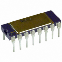
IC MULT/DIV DUAL CH LIN 16-CDIP
Manufacturer
Analog Devices Inc
Specifications of AD539JD
Rohs Status
RoHS non-compliant
Function
Analog Multiplier/Divider
Number Of Bits/stages
2
Package / Case
16-CDIP (0.300", 7.62mm)
Number Of Elements
2
Output Type
Single
Power Supply Requirement
Dual
Single Supply Voltage (typ)
Not RequiredV
Single Supply Voltage (min)
Not RequiredV
Single Supply Voltage (max)
Not RequiredV
Dual Supply Voltage (typ)
±5/±9/±12V
Dual Supply Voltage (min)
±4.5V
Dual Supply Voltage (max)
±15V
Operating Temperature Classification
Commercial
Mounting
Through Hole
Pin Count
16
Package Type
SBCDIP
Lead Free Status / RoHS Status
Not Compliant
Available stocks
Company
Part Number
Manufacturer
Quantity
Price

Part Number:
AD539JD
Manufacturer:
ADI/亚德诺
Quantity:
20 000


BASIC DIVIDER CONNECTIONS
Standard Scaling
The AD539 provides excellent operation as a two-quadrant
analog divider in wideband, wide gain-range applications, with
the advantage of dual-channel operation. Figure 25 shows the
simplest connections for division with a transfer function of
Recalling that the nominal value of V
simplified to
where all signals are expressed in volts. The circuit thus exhibits
unity gain for V
The output swing is limited to ±2 V nominal full scale and ±4.2 V
peak (using a −V
Because the maximum loss is 10 dB (at V
that the maximum input to V
low distortion applications and no more than ±13.4 V (9.5 V
AD539
V
V
Y
Y
= −V
= −V
U
W
V
/V
W
X
X
/V
S
= 1 V and a gain of 40 dB when V
supply of at least 7.5 V for the AD539).
X
DENOMINATOR
NOTES
1. DECOUPLE OP AMP SUPPLIES.
INPUT, V
W
should be ±6.3 V (4.4 V rms) for
X
Figure 25. 2-Channel Divider with 1 V Scaling (16-Lead SBDIP and PDIP Shown)
U
is 1 V, this can be
X
= 3.162 V), it follows
0.47µF
0.47µF
C
X
–7.5V
C
+5V
= 0.01 V.
= 3nF
1
2
3
4
5
6
7
8
Rev. B | Page 16 of 20
V
HF COMP
V
+V
–V
V
INPUT
COMMON
OUTPUT
COMMON
X
Y1
Y2
S
S
AD539
COMMON
OUTPUT
OUTPUT
BASE
CHAN1
CHAN2
rms) to avoid clipping. Note that offset adjustment is needed for
the op amps to maintain accurate dc levels at the output in high
gain applications: the noise gain is 6 V/V
The gain magnitude response for this configuration using the
LH0032 op amps with nominally 12 pF compensation (HF
COMP, Pin 2, to V
however, other amplifiers can also be used. Because there is some
manufacturing variation in the HF response of the op amps and
load conditions also affect the response, these capacitors should
be adjustable: 5 pF to 15 pF is recommended for both positions.
The bandwidth in this configuration is nominally 17 MHz at
V
35 kHz at V
the use of a good ground plane and power supply decoupling
should be carefully observed. Other suitable high speed op amps
include: AD844, AD827, and AD811. Consult these data sheets
for suitable applications circuits.
W1
W2
Z2
Z1
X
NUMERATOR 1
NUMERATOR 2
= 3.162 V, 4.5 MHz at V
16
15
14
13
12
10
11
9
NC
NC
V
V
W1
W2
X
= 0.01 V. The general recommendations regarding
2pF TO 15pF
2pF TO 15pF
2pF TO
15pF
2pF TO
15pF
2
2
LH0032
Y1
, Pin 3) and C
3
3
X
= 1 V, 350 kHz at V
V
V
Y1
Y2
= –
= –
F
= 7 pF is shown in Figure 17;
V
V
V
V
W1
W2
X
X
X
, or 600 at V
X
= 0.1 V, and
X
= 0.01 V.
Related parts for AD539JD
Image
Part Number
Description
Manufacturer
Datasheet
Request
R

Part Number:
Description:
±1.7g Dual-Axis IMEMS Accelerometer Evaluation Board
Manufacturer:
Analog Devices Inc
Datasheet:

Part Number:
Description:
Inertial Sensor Evaluation System
Manufacturer:
Analog Devices Inc
Datasheet:
Part Number:
Description:
Manufacturer:
Analog Devices Inc
Datasheet:
Part Number:
Description:
Manufacturer:
Analog Devices Inc
Datasheet:
Part Number:
Description:
Manufacturer:
Analog Devices Inc
Datasheet:
Part Number:
Description:
Manufacturer:
Analog Devices Inc
Datasheet:
Part Number:
Description:
Manufacturer:
Analog Devices Inc
Datasheet:
Part Number:
Description:
Manufacturer:
Analog Devices Inc
Datasheet:
Part Number:
Description:
Manufacturer:
Analog Devices Inc
Datasheet:
Part Number:
Description:
Manufacturer:
Analog Devices Inc
Datasheet:
Part Number:
Description:
Manufacturer:
Analog Devices Inc
Datasheet:
Part Number:
Description:
Manufacturer:
Analog Devices Inc
Datasheet:
Part Number:
Description:
Manufacturer:
Analog Devices Inc
Datasheet: