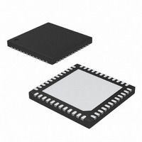
DS3514T+T&R Maxim Integrated Products, DS3514T+T&R Datasheet - Page 5

DS3514T+T&R
Manufacturer Part Number
DS3514T+T&R
Description
IC I2C GAMMA/VCOM BUFF 48-TQFN
Manufacturer
Maxim Integrated Products
Datasheet
1.DS3514TTR.pdf
(21 pages)
Specifications of DS3514T+T&R
Applications
TFT-LCD Panels: Gamma Buffer, VCOM Driver
Output Type
Rail-to-Rail
Number Of Circuits
14
Current - Supply
5mA
Current - Output / Channel
4mA
Voltage - Supply, Single/dual (±)
9 V ~ 15 V
Mounting Type
Surface Mount
Package / Case
48-TQFN Exposed Pad
Lead Free Status / RoHS Status
Lead free / RoHS Compliant
NONVOLATILE MEMORY CHARACTERISTICS
(V CC = +2.7V to +5.5V.)
Note 1:
Note 2:
Note 3:
Note 4:
Note 5:
Note 6:
Note 7:
Note 8:
Note 9:
Note 10: Differential nonlinearity is the deviation of the step-size change between two LSB settings from the expected step size. The
Note 11: Specified with the V
Note 12: EEPROM data is assumed already settled at input of Latch B. LD transitions after EEPROM byte has been selected.
Note 13: Rising transition from 5V to 10V; falling transition from 10V to 5V.
Note 14: I
Note 15: C
Note 16: EEPROM write time begins after a STOP condition occurs.
Note 17: Pulses narrower than max are suppressed.
Figure 1. V
EEPROM Write Cycles
All voltages are referenced to ground. Currents entering the IC are specified positive and currents exiting the IC are
negative.
If V
devices on the I
I
I
I
I
This is the minimum V
This is the time from V
Integral nonlinearity is the deviation of a measured value from the expected values at each particular setting. Expected
value is calculated by connecting a straight line from the measured minimum setting to the measured maximum setting.
INL = [V(RW)
expected LSB step size is the slope of the straight line from measured minimum position to measured maximum position.
DNL = [V(RW)
standard-mode timing.
PARAMETER
COM
DD
CC
CCQ
DDQ
2
C interface timing shown is for fast-mode (400kHz) operation. This device is also backward-compatible with I
B
—total capacitance of one bus line in picofarads.
CC
I
supply current is specified with V
is specified with the following conditions: SCL = 400kHz, SDA = V
2
is specified with the following conditions: SCL = SDA = V
is specified with the following conditions: SCL = SDA = V
Settling Timing Diagram
is less than +2.7V or is left unconnected, the DS3514 pulls the I
C Gamma and V
_______________________________________________________________________________________
80h
i
- (V(RW)
i+1
2
C bus.
- (V(RW)
COM
CC
CC
0
VRH
VRL
8-BIT
]/LSB(measured) - i, for i = 0...N (N = 255 for V
DAC
and gamma bias currents set to 100% (CR.5 = 1, CR.4 = 0).
voltage that causes EEPROM to be recalled.
> V
i
SYMBOL
]/LSB(measured) - 1, for i = 0...(N - 1) (N = 255 for V
POR
DS3514
V
and V
COM
DD
T
T
DD
A
A
= 15.0V and no load on V
= +85°C (Guaranteed by design)
= +25°C (Guaranteed by design)
> V
V
DD
DD(MIN)
COM
CONDITIONS
until the device is powered up.
V
COM
CC
CC
= 5.5V, and V
= 5.5V and V
COM
Buffer with EEPROM
C
D
CC
= 1μF
2
COM
C bus to V
or GM1–GM14 outputs.
2.2Ω
= 5.5V, and V
, 1023 for GM1–GM14).
COM
COM
COM
CC
0.1μF
, 1023 for GM1–GM14).
and GM1–GM14 floating.
, preventing communication with other
and GM1–GM14 floating.
COM
200,000
50,000
MIN
and GM1–GM14 floating.
0 TO 1.5V
50kHz
MAX
2
C
UNITS
Writes
5


