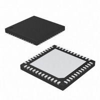
DS3514T+T&R Maxim Integrated Products, DS3514T+T&R Datasheet - Page 16

DS3514T+T&R
Manufacturer Part Number
DS3514T+T&R
Description
IC I2C GAMMA/VCOM BUFF 48-TQFN
Manufacturer
Maxim Integrated Products
Datasheet
1.DS3514TTR.pdf
(21 pages)
Specifications of DS3514T+T&R
Applications
TFT-LCD Panels: Gamma Buffer, VCOM Driver
Output Type
Rail-to-Rail
Number Of Circuits
14
Current - Supply
5mA
Current - Output / Channel
4mA
Voltage - Supply, Single/dual (±)
9 V ~ 15 V
Mounting Type
Surface Mount
Package / Case
48-TQFN Exposed Pad
Lead Free Status / RoHS Status
Lead free / RoHS Compliant
I
16
Control Register 48h: Control Register (CR)
FACTORY DEFAULT
MEMORY TYPE
Bits 7:6
Bits 5:4
Bits 3:2
Bits 1:0
Status Bits Register 4Ah: Real-Time Indicator of Logic State on LD, S1, and S0 Pins
FACTORY DEFAULT
MEMORY TYPE
GDATx Register: EEPROM Data for the Gamma Channels
This is an example of how the bits are arranged for a typical GDATx memory location. GDATx has 10 bits that are
arranged in two consecutive bytes. The following example shows the arrangement for GM1 GDAT1 (58h–59h). This
arrangement is applicable for all the EEPROM data for all gamma channels.
FACTORY DEFAULT
MEMORY TYPE
2
C Gamma and V
______________________________________________________________________________________
4Ah
48h
58h
59h
Reserved
V
00 = 60%
01 = 80%
10 = 100% (default)
11 = 150%
Reserved
DS3514 Mode (MODE[1:0]):
00 = S0/S1 pins are used to select the desired bank (A–D) (default).
01 = SOFT S0/S1 (bits) are used to select the desired bank (A–D).
1X = Latch A is used to control the DACs.
COM
GDAT[9]
GDAT[1]
BIT 7
BIT 7
BIT 7
LD
x
and Gamma Bias Current Control Bits (BIAS[1:0]):
GDAT[8]
GDAT[0]
x
x
20h
NV
—
Read Only
8000h
NV
COM
GDAT[7]
BIAS1
x
x
Buffer with EEPROM
GDAT[6]
BIAS0
x
x
GDAT[5]
x
x
x
GDAT[4]
x
x
x
GDAT[3]
MODE1
S1
x
GDAT[2]
MODE0
BIT 0
BIT 0
BIT 0
S0
x


