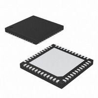
DS3514T+T&R Maxim Integrated Products, DS3514T+T&R Datasheet - Page 13

DS3514T+T&R
Manufacturer Part Number
DS3514T+T&R
Description
IC I2C GAMMA/VCOM BUFF 48-TQFN
Manufacturer
Maxim Integrated Products
Datasheet
1.DS3514TTR.pdf
(21 pages)
Specifications of DS3514T+T&R
Applications
TFT-LCD Panels: Gamma Buffer, VCOM Driver
Output Type
Rail-to-Rail
Number Of Circuits
14
Current - Supply
5mA
Current - Output / Channel
4mA
Voltage - Supply, Single/dual (±)
9 V ~ 15 V
Mounting Type
Surface Mount
Package / Case
48-TQFN Exposed Pad
Lead Free Status / RoHS Status
Lead free / RoHS Compliant
or exceeds +150°C. In this state, the V
disabled (output goes high impedance) until the junc-
tion temperature falls below +150°C.
The slave address byte consists of a 7-bit slave
address plus a R/W bit (see Figure 5). The DS3514’s
slave address is determined by the state of the A0 pin.
This pin allows up to two devices to reside on the same
I
corresponding bit position in the slave address.
Conversely, connecting A0 to V
corresponding bit position. For example, the DS3514’s
slave address byte is C0h when A0 is grounded. I
communication is described in detail in the I
Interface Description section.
The list of registers/memory contained in the DS3514 is
shown in the Memory Map section. Also shown for
each of the registers is the memory type, accessibility,
2
C bus. Connecting A0 to GND results in a 0 in the
Latch A for GM10 Ch
Latch A for GM11 Ch
Latch A for GM12 Ch
Latch A for V
Latch A for GM1 Ch
Latch A for GM2 Ch
Latch A for GM3 Ch
Latch A for GM4 Ch
Latch A for GM5 Ch
Latch A for GM6 Ch
Latch A for GM7 Ch
Latch A for GM8 Ch
Latch A for GM9 Ch
Slave Address Byte and Address Pin
NAME
I
2
COM
C Gamma and V
______________________________________________________________________________________
Ch
Memory Organization
10h, 11h
12h, 13h
14h, 15h
16h, 17h
18h, 19h
Ah, Bh
Ch, Dh
2h, 3h
4h, 5h
6h, 7h
8h, 9h
Eh, Fh
(HEX)
0h
Memory Description
ADDRESS
CC
results in a 1 in the
(DEC)
10, 11
12, 13
14, 15
16, 17
18, 19
20, 21
22, 23
24, 25
2, 3
4, 5
6, 7
8, 9
0
COM
2
buffer is
C Serial
8-Bit I
10-Bit I
10-Bit I
10-Bit I
10-Bit I
10-Bit I
10-Bit I
10-Bit I
10-Bit I
10-Bit I
10-Bit I
10-Bit I
10-Bit I
2
2
C
C Data for V
2
2
2
2
2
2
2
2
2
2
2
2
C Data for GM1 DAC
C Data for GM2 DAC
C Data for GM3 DAC
C Data for GM4 DAC
C Data for GM5 DAC
C Data for GM6 DAC
C Data for GM7 DAC
C Data for GM8 DAC
C Data for GM9 DAC
C Data for GM10 DAC
C Data for GM11 DAC
C Data for GM12 DAC
COM
DESCRIPTION
as well as the power-up default values for volatile loca-
tions and factory-programmed defaults for the non-
volatile locations. Additional information regarding
reading and writing the memory is located in the I
Serial Interface Description section.
Figure 5. DS3514 Slave Address Byte
COM
Buffer with EEPROM
*THE SLAVE ADDRESS IS DETERMINED BY ADDRESS PIN A0.
DAC
MSB
1
1
SLAVE ADDRESS*
0
OR COMMAND
0
MEMORY
Volatile
Volatile
Volatile
Volatile
Volatile
Volatile
Volatile
Volatile
Volatile
Volatile
Volatile
Volatile
Volatile
TYPE
0
0
Memory Map
A0
ACCESS
LSB
R/W
R/W
R/W
R/W
R/W
R/W
R/W
R/W
R/W
R/W
R/W
R/W
R/W
R/W
I
2
C
2
13
C


