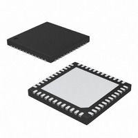
DS3514T+T&R Maxim Integrated Products, DS3514T+T&R Datasheet - Page 17

DS3514T+T&R
Manufacturer Part Number
DS3514T+T&R
Description
IC I2C GAMMA/VCOM BUFF 48-TQFN
Manufacturer
Maxim Integrated Products
Datasheet
1.DS3514TTR.pdf
(21 pages)
Specifications of DS3514T+T&R
Applications
TFT-LCD Panels: Gamma Buffer, VCOM Driver
Output Type
Rail-to-Rail
Number Of Circuits
14
Current - Supply
5mA
Current - Output / Channel
4mA
Voltage - Supply, Single/dual (±)
9 V ~ 15 V
Mounting Type
Surface Mount
Package / Case
48-TQFN Exposed Pad
Lead Free Status / RoHS Status
Lead free / RoHS Compliant
The following terminology is commonly used to
describe I
Electrical Characteristics for additional information.)
Master device: The master device controls the
slave devices on the bus. The master device gener-
ates SCL clock pulses and START and STOP condi-
tions.
Slave devices: Slave devices send and receive
data at the master’s request.
Bus idle or not busy: Time between STOP and
START conditions when both SDA and SCL are inac-
tive and in their logic-high states.
START condition: A START condition is generated
by the master to initiate a new data transfer with a
slave. Transitioning SDA from high to low while SCL
remains high generates a START condition.
STOP condition: A STOP condition is generated by
the master to end a data transfer with a slave.
Transitioning SDA from low to high while SCL
remains high generates a STOP condition.
Repeated START condition: The master can use a
repeated START condition at the end of one data
transfer to indicate that it will immediately initiate a
new data transfer following the current one.
Repeated STARTs are commonly used during read
operations to identify a specific memory address to
begin a data transfer. A repeated START condition
is issued identically to a normal START condition.
Bit write: Transitions of SDA must occur during the
low state of SCL. The data on SDA must remain valid
and unchanged during the entire high pulse of SCL
plus the setup and hold time requirements. Data is
shifted into the device during the rising edge of the
SCL.
Bit read: At the end of a write operation, the master
must release the SDA bus line for the proper amount
of setup time before the next rising edge of SCL dur-
ing a bit read. The device shifts out each bit of data
on SDA at the falling edge of the previous SCL pulse
and the data bit is valid at the rising edge of the cur-
rent SCL pulse. Remember that the master gener-
ates all SCL clock pulses, including when it is
reading bits from the slave.
Acknowledge (ACK and NACK): An Acknowledge
(ACK) or Not Acknowledge (NACK) is always the 9th
bit transmitted during a byte transfer. The device
receiving data (the master during a read or the slave
I
2
C Serial Interface Description
2
C data transfers. (See Figure 4 and the I
I
2
C Gamma and V
______________________________________________________________________________________
I
2
C Definitions
2
C
COM
during a write operation) performs an ACK by trans-
mitting a 0 during the 9th bit. A device performs a
NACK by transmitting a 1 during the 9th bit. Timing
for the ACK and NACK is identical to all other bit
writes. An ACK is the acknowledgment that the
device is properly receiving data. A NACK is used to
terminate a read sequence or indicates that the
device is not receiving data.
Byte write: A byte write consists of 8 bits of informa-
tion transferred from the master to the slave (most
significant bit first) plus a 1-bit acknowledgment
from the slave to the master. The 8 bits transmitted
by the master are done according to the bit-write
definition and the acknowledgment is read using the
bit-read definition.
Byte read: A byte read is an 8-bit information trans-
fer from the slave to the master plus a 1-bit ACK or
NACK from the master to the slave. The 8 bits of
information that are transferred (most significant bit
first) from the slave to the master are read by the
master using the bit read definition, and the master
transmits an ACK using the bit write definition to
receive additional data bytes. The master must
NACK the last byte read to terminate communication
so the slave will return control of SDA to the master.
Slave address byte: Each slave on the I
responds to a slave address byte sent immediately
following a START condition. The slave address byte
contains the slave address in the most significant 7
bits and the R/W bit in the least significant bit.
The DS3514’s slave address is determined by the
state of the A0 address pin as shown in Figure 5. An
address pin connected to GND results in a 0 in the
corresponding bit position in the slave address.
Conversely, an address pin connected to V
results in a 1 in the corresponding bit position.
When the R/W bit is 0 (such as in C0h), the master is
indicating it will write data to the slave. If R/W is set
to a 1 (C1h in this case), the master is indicating that
it wants to read from the slave.
If an incorrect (nonmatching) slave address is writ-
ten, the DS3514 assumes the master is communicat-
ing with another I
communication until the next START condition is
sent.
Memory address: During an I
the DS3514, the master must transmit a memory
address to identify the memory location where the
slave is to store the data. The memory address is
always the second byte transmitted during a write
operation following the slave address byte.
Buffer with EEPROM
2
C device and ignores the
2
C write operation to
2
C bus
CC
17


