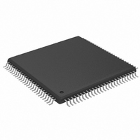
MAX2038CCQ+ Maxim Integrated Products, MAX2038CCQ+ Datasheet - Page 6

MAX2038CCQ+
Manufacturer Part Number
MAX2038CCQ+
Description
IC VGA W/OCTAL MIXER 8CH 100TQFP
Manufacturer
Maxim Integrated Products
Type
Variable Gain Amplifierr
Datasheet
1.MAX2038CCQT.pdf
(24 pages)
Specifications of MAX2038CCQ+
Applications
Medical Ultrasound Imaging, Sonar
Mounting Type
Surface Mount
Package / Case
100-TQFP Exposed Pad, 100-eTQFP, 100-HTQFP, 100-VQFP
Lead Free Status / RoHS Status
Lead free / RoHS Compliant
Ultrasound VGA Integrated
with CW Octal Mixer
AC ELECTRICAL CHARACTERISTICS—CW MIXER MODE (continued)
( Typical Application Circuit , Figure 7. V
CW_FILTER = 1, TEST_MODE = 0, PD = 0, CW_VG = 0, CW_M1 = 0, CW_M2 = 0, VG_CLAMP_MODE = 1, f
capacitance to GND at each of the VGA differential outputs is 60pF, differential capacitance across the VGA outputs is 10pF, R
1kΩ, CW mixer outputs pulled up to +11V through four separate ±0.1% 115Ω resistors, differential mixer inputs are driven from a low
impedance source. Typical values are at V
Note 2: Specifications at T
Note 3: Noise performance of the device is dependent on the noise contribution from the supply to V
Note 4: Total on-chip power dissipation is calculated as P
Note 5: Note that the LVDS CWD LO clocks are DC-coupled. This is to ensure immediate synchronization when the clock is first
Note 6: External 100Ω resistor terminates the LVDS differential signal path.
Note 7: The mixer common-mode current (3.25mA/channel) is specified as the common-mode current in each of the differential
Note 8: Specification guaranteed only for DOUT driving DIN of the next device in a daisy-chain fashion.
Note 9: This response time does not include the CW output highpass filter. When switching to VGA mode, the CW outputs stop
Note 10: See the Ultrasound-Specific IMD3 Specification in the Applications Information section.
Note 11: Mixer output-voltage compliance is the range of acceptable voltages allowed on the CW mixer outputs.
Note 12: Channel-to-channel gain-and-phase matching measured on 30 pieces during engineering characterization at room tem-
Note 13: Transconductance is defined as the quadrature summing of the CW differential output current at baseband divided by the
6
SERIAL SHIFT REGISTER
Serial Shift Register
Programming Rate
Minimum Data Set-Up Time
Minimum Data Hold Time
Minimum Data Clock Time
Minimum Data Clock Pulse Width
High
Minimum Data Clock Pulse Width
Low
Minimum Load Line
Minimum Load Line High to
Mixer Clock On
Minimum Data Clock to Load
Line High
_______________________________________________________________________________________
teed by design and characterization.
V
turned on. An AC-coupled LO is problematic in that the RC time constant associated with the coupling capacitors and the
input impedance of the pin causes there to be a period of time (related to the RC time constant) when the DC level on the
chip side of the capacitor is outside the acceptable common-mode range and the LO swing does not exceed both the
logic thresholds required for proper operation. This problem associated with AC-coupling would cause an inability to
ensure synchronization among beam-forming channels. The LVDS signal is terminated differentially with an external 100Ω
resistor on the board.
mixer outputs (CW_QOUT+, CW_QOUT-, CW_IOUT+, CW_IOUT-).
drawing current and the output voltage goes to the rail. If a highpass filter is used, the recovery time can be excessive and
a switching network is recommended as shown in the Applications Information section.
perature. Each mixer is used as a phase detector and produces a DC voltage in the IQ plane. The phase is given by the
angle of the vector drawn on that plane. Multiple channels from multiple parts are compared to each other to produce the
phase variation.
mixer’s input voltage.
PARAMETER
REF
. V
CC
and V
REF
A
can be connected together to share the same supply voltage if the supply for V
= +25°C and T
t
SYMBOL
t
DCLKPWH
DCLKPWL
t
MIXCLK
t
t
t
DCLK
t
DSU
HLD
CLH
CC
t
LD
CC
= V
= V
A
REF
= +70°C are guaranteed by production test. Specifications at T
REF
= 4.75V to 5.25V, T
= 5V, T
DISS
A
= +25°C, unless otherwise noted.) (Note 2)
CONDITIONS
= V
CC
x I
A
CC
= 0°C to +70°C, V
+ V
REF
x I
REF
+ [11V - (I
GND
MIN
= 0V, LOW_PWR = 0, M4_EN = 0,
MIX
REF
/4) x 115] x I
. Use a low-noise supply for
TYP
100
30
30
30
30
30
30
2
CC
exhibits low noise.
RF
A
= 0°C are guaran-
= f
MAX
MIX
10
LO
.
/16 = 5MHz,
UNITS
MHz
ns
ns
ns
ns
ns
ns
ns
ns
L
=


