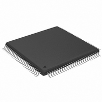
MAX2038CCQ+ Maxim Integrated Products, MAX2038CCQ+ Datasheet - Page 17

MAX2038CCQ+
Manufacturer Part Number
MAX2038CCQ+
Description
IC VGA W/OCTAL MIXER 8CH 100TQFP
Manufacturer
Maxim Integrated Products
Type
Variable Gain Amplifierr
Datasheet
1.MAX2038CCQT.pdf
(24 pages)
Specifications of MAX2038CCQ+
Applications
Medical Ultrasound Imaging, Sonar
Mounting Type
Surface Mount
Package / Case
100-TQFP Exposed Pad, 100-eTQFP, 100-HTQFP, 100-VQFP
Lead Free Status / RoHS Status
Lead free / RoHS Compliant
The LO_LVDS input frequency is 8 x f
2 operation. The CWD LO frequency range is 1MHz to
7.5MHz, and the input frequency ranges from 8MHz to
60MHz. This high LO clock frequency requires a differ-
ential LVDS input. The 8 x f
to produce 8 phases. These 8 phases are generated
for each of the 8 channels and programmed for the
selected phase by the serial shift register. Note that the
serial shift register is common to modes 1, 2, 3, and
where each channel has a corresponding 5-bit shift
register, which is used to program the output phase.
However, since mode 2 generates 8 phases only, 3 of
the 4 phase-programming bits are used; 5 bits are still
loaded per channel using the serial shift register, but
the phase-programming MSB is a don’t-care bit. The
fifth bit in the shift register always turns each channel
on/off individually. For mode 2, set CW_M1 to a logic-
low and set CW_M2 to a logic-high. See Table 3.
The LO_LVDS input is not used in this mode. Separate
4 x f
each channel. The CWD LO frequency range is 1MHz
to 7.5MHz, and the input frequency provides ranges
from 4MHz to 30MHz. Note that the LO clock frequency
can utilize 3V CMOS inputs. The 4 x f
inputs are divided by 4 to produce 4 phases. These
4 phases are generated for each of the 8 channels and
Table 3. Mode 2 Logic Table (DC = Don’t
Care, B4 = 0: Channel On/B4 = 1: Channel
Off)
CW_M1 = 0
CW_M2 = 1
MODE 2
PHASE
(DEG)
135
180
225
270
315
LO
45
90
0
clock inputs are provided using LO1–LO8 for
MSB
(B0)
DC
DC
DC
DC
DC
DC
DC
DC
D
______________________________________________________________________________________
(B1)
C
0
0
0
0
1
1
1
1
LO
(B2)
B
input is then divided by 8
0
0
1
1
0
0
1
1
LSB
(B3)
A
LO
0
1
0
1
0
1
0
1
(typ) for mode
LO
SHUTDOWN
LO1–LO8
(B4)
Mode 2
SD
0/1
0/1
0/1
0/1
0/1
0/1
0/1
0/1
Mode 3
Ultrasound VGA Integrated
programmed for the selected phase by the serial shift
register. For mode 3, 4 phases are generated, and only
2 of the 4 phase-programming bits are required where
the 2-phase programming MSBs are “don’t-care” bits.
For mode 3, set CW_M1 to a logic-high and set CW_M2
to a logic-low. See Table 4.
The LO_LVDS input is not used in this mode. The
appropriate phases are externally provided using sepa-
rate 4 x f
input is required so the device can internally generate
accurate duty-cycle independent quadrature LO drives.
Note that the serial shift register is not used in this
mode. The CWD LO frequency range is 1MHz to
7.5MHz and the input frequency ranges from 4MHz to
30MHz. The appropriate inputs are provided at LO1 to
LO8. A reset line is provided to the customer so that
they can synchronize all the CWD channels. The reset
line is implemented through the RESET. For mode 4, set
both CW_M1 and CW_M2 to logic-high. See Table 5.
Table 4. Mode 3 Logic Table (DC = Don’t
Care, B4 = 0: Channel On/B4 = 1: Channel
Off)
Table 5. Mode 4 Logic Table
N/A = Not applicable.
Serial bus
not used in
mode 4
CW_M1 = 1
CW_M2 = 0
CW_M1 = 1
CW_M2 = 1
MODE 3
MODE 4
PHASE
PHASE
(DEG)
(DEG)
180
270
90
0
with CW Octal Mixer
LO
LO1–LO8 inputs for each channel. A 4 x f
MSB
(B0)
MSB
DC
DC
DC
DC
(B0)
N/A
D
D
(B1)
DC
DC
DC
DC
(B1)
N/A
C
C
(B2)
(B2)
N/A
B
0
0
1
1
B
LSB
(B3)
LSB
(B3)
N/A
A
0
1
0
1
A
SHUTDOWN
SHUTDOWN
(B4)
(B4)
Mode 4
SD
0/1
0/1
0/1
0/1
N/A
SD
17
LO


