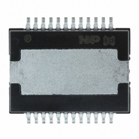
TDF8590TH/N1,118 NXP Semiconductors, TDF8590TH/N1,118 Datasheet - Page 9

TDF8590TH/N1,118
Manufacturer Part Number
TDF8590TH/N1,118
Description
IC AMP AUDIO PWR 160W D 24HSOP
Manufacturer
NXP Semiconductors
Type
Class Dr
Datasheet
1.TDF8590THN1S118.pdf
(30 pages)
Specifications of TDF8590TH/N1,118
Output Type
1-Channel (Mono) or 2-Channel (Stereo)
Package / Case
24-HSOP
Max Output Power X Channels @ Load
160W x 1 @ 8 Ohm; 80W x 2 @ 4 Ohm
Voltage - Supply
±14 V ~ 29 V
Features
Depop, Differential Inputs, Mute, Short-Circuit and Thermal Protection, Standby
Mounting Type
Surface Mount
Product
Class-D
Output Power
160 W
Available Set Gain
32 dB
Common Mode Rejection Ratio (min)
75 dB
Thd Plus Noise
0.15 %
Maximum Operating Temperature
+ 85 C
Mounting Style
SMD/SMT
Audio Load Resistance
8 Ohms
Dual Supply Voltage
+/- 27 V
Input Signal Type
Differential
Minimum Operating Temperature
- 40 C
Output Signal Type
Differential, Single
Supply Type
Dual
Lead Free Status / RoHS Status
Lead free / RoHS Compliant
Other names
935278835118
TDF8590TH/N1-T
TDF8590TH/N1-T
TDF8590TH/N1-T
TDF8590TH/N1-T
NXP Semiconductors
TDF8590TH_2
Product data sheet
6.5 Diagnostic output
6.6 Differential inputs
[3]
[4]
Pin DIAG is pulled LOW when the OCP is triggered. With a continuous shorted load a
switching pattern in the voltage on pin DIAG is observed (see
LOW on pin DIAG indicates a short to the supply lines whereas a shorted load causes a
switching DIAG pin (see
The pin DIAG reference voltage is V
pull-up. An example of a circuit to read out and level shift the diagnostic data is given in
Figure
microprocessor that reads out the DIAG data.
For a high Common Mode Rejection Ratio (CMRR) and a maximum of flexibility in the
application, the audio inputs are fully differential. By connecting the inputs anti-parallel the
phase of one of the channels can be inverted, so that a load can be connected between
the two output filters. In this case the system operates as a mono BTL amplifier.
The input configuration for a mono BTL application is illustrated in
In the stereo SE configuration it is also recommended to connect the two differential
inputs in anti-phase. This has advantages for the current handling of the power supply at
low signal frequencies (supply pumping).
Fig 7. DIAG readout circuit with level shift
Only complete shut down of amplifier in case of a short-circuit. In all other cases current limiting resulting in
clipping output signal.
Fault condition detected during (every) transition between standby-to-mute and during restart after
activation of OCP (short to one of the supply lines).
7. V5V represents a logic supply that is used in the application by the
Rev. 02 — 23 April 2007
Section
V
DIAG
V
DDA
SSA
2
80 W SE (4 ) or 1
6.4.3).
100 k
SSA
. Pin DIAG should not be connected to an external
5.6 V
M1
100 k
27 k
SGND
V5V
160 W BTL (8 ) class-D amplifier
M2
10 k
001aad840
DIAG
out
Figure
TDF8590TH
Figure
6). A permanent
© NXP B.V. 2007. All rights reserved.
8.
9 of 30


