TDF8590TH/N1,118 NXP Semiconductors, TDF8590TH/N1,118 Datasheet - Page 17

TDF8590TH/N1,118
Manufacturer Part Number
TDF8590TH/N1,118
Description
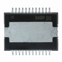
IC AMP AUDIO PWR 160W D 24HSOP
Manufacturer
NXP Semiconductors
Type
Class Dr
Datasheet
1.TDF8590THN1S118.pdf
(30 pages)
Specifications of TDF8590TH/N1,118
Output Type
1-Channel (Mono) or 2-Channel (Stereo)
Package / Case
24-HSOP
Max Output Power X Channels @ Load
160W x 1 @ 8 Ohm; 80W x 2 @ 4 Ohm
Voltage - Supply
±14 V ~ 29 V
Features
Depop, Differential Inputs, Mute, Short-Circuit and Thermal Protection, Standby
Mounting Type
Surface Mount
Product
Class-D
Output Power
160 W
Available Set Gain
32 dB
Common Mode Rejection Ratio (min)
75 dB
Thd Plus Noise
0.15 %
Maximum Operating Temperature
+ 85 C
Mounting Style
SMD/SMT
Audio Load Resistance
8 Ohms
Dual Supply Voltage
+/- 27 V
Input Signal Type
Differential
Minimum Operating Temperature
- 40 C
Output Signal Type
Differential, Single
Supply Type
Dual
Lead Free Status / RoHS Status
Lead free / RoHS Compliant
Other names
935278835118
TDF8590TH/N1-T
TDF8590TH/N1-T
TDF8590TH/N1-T
TDF8590TH/N1-T
NXP Semiconductors
TDF8590TH_2
Product data sheet
12.5 Heat sink requirements
12.6 Pumping effects
In some applications it may be necessary to connect an external heat sink to the
TDF8590TH. The thermal foldback activates on T
the relationship between the maximum power dissipation before activation of the thermal
foldback and the total thermal resistance from junction to ambient:
The power dissipation is determined by the efficiency
measured as a function of output power is given in
be derived as function of output power (see
Example of a heatsink calculation for the 8
When the TDF8590TH is used in a SE configuration, a so-called pumping effect can
occur. During one switching interval, energy is taken from one supply (e.g. V
part of that energy is delivered back to the other supply line (e.g. V
When the voltage supply source cannot sink energy, the voltage across the output
capacitors of that voltage supply source will increase: the supply voltage is pumped to
higher levels. The voltage increase caused by the pumping effect depends on:
R
•
•
•
•
•
•
•
•
•
•
•
•
th j a –
An audio signal with a crest factor of 10 (the ratio between peak power and average
power is 10 dB), this means that the average output power is 1/10th of the peak power
The peak RMS output power level is 130 W (0.5 % THD level)
The average power is 0.1
The dissipated power at an output power of 13 W is approximately 5 W
The total R
The total thermal resistance R
R
would then be: 11
Speaker impedance
Supply voltage
Audio signal frequency
Value of decoupling capacitors on supply lines
Source and sink currents of other channels
th(j-c)
=
= 1.1 K/W, R
T
----------------------- -
j
–
P
th(j-a)
T
amb
= (140
th(c-h)
Rev. 02 — 23 April 2007
(1.1 + 1) = 8.9 K/W
2
= 0.5 K/W to 1 K/W (dependent on mounting), so R
85) / 5 = 11 K/W, if the maximum expected T
80 W SE (4 ) or 1
130 W = 13 W
th(j-a)
= R
th(j-c)
Figure
BTL application with 27 V supply:
+ R
j
= 140 C. The expression below shows
Figure
24).
th(c-h)
160 W BTL (8 ) class-D amplifier
of the TDF8590TH. The efficiency
+ R
23. The power dissipation can
th(h-a)
TDF8590TH
SSA1
© NXP B.V. 2007. All rights reserved.
) and visa versa.
amb
DDA1
= 85 C
), while a
th(h-a)
17 of 30


