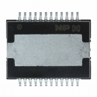
TDF8590TH/N1,118 NXP Semiconductors, TDF8590TH/N1,118 Datasheet - Page 7

TDF8590TH/N1,118
Manufacturer Part Number
TDF8590TH/N1,118
Description
IC AMP AUDIO PWR 160W D 24HSOP
Manufacturer
NXP Semiconductors
Type
Class Dr
Datasheet
1.TDF8590THN1S118.pdf
(30 pages)
Specifications of TDF8590TH/N1,118
Output Type
1-Channel (Mono) or 2-Channel (Stereo)
Package / Case
24-HSOP
Max Output Power X Channels @ Load
160W x 1 @ 8 Ohm; 80W x 2 @ 4 Ohm
Voltage - Supply
±14 V ~ 29 V
Features
Depop, Differential Inputs, Mute, Short-Circuit and Thermal Protection, Standby
Mounting Type
Surface Mount
Product
Class-D
Output Power
160 W
Available Set Gain
32 dB
Common Mode Rejection Ratio (min)
75 dB
Thd Plus Noise
0.15 %
Maximum Operating Temperature
+ 85 C
Mounting Style
SMD/SMT
Audio Load Resistance
8 Ohms
Dual Supply Voltage
+/- 27 V
Input Signal Type
Differential
Minimum Operating Temperature
- 40 C
Output Signal Type
Differential, Single
Supply Type
Dual
Lead Free Status / RoHS Status
Lead free / RoHS Compliant
Other names
935278835118
TDF8590TH/N1-T
TDF8590TH/N1-T
TDF8590TH/N1-T
TDF8590TH/N1-T
NXP Semiconductors
TDF8590TH_2
Product data sheet
When the loudspeaker terminals are short-circuited and the OCP is triggered the
TDF8590TH is switched off completely and will try to restart every 100 ms (see
A short of the loudspeaker terminals to one of the supply lines will also trigger the
activation of the OCP and the amplifier will shut down. During restart the window
protection will be activated. As a result the amplifier will not start up after 100 ms and pin
DIAG will remain LOW until the short to the supply lines is removed.
Fig 5. Pin DIAG with activated current limiting
Fig 6. Restart of the TDF8590TH
•
•
•
50 ms after switch off pin DIAG will be released
100 ms after switch off the amplifier will return to mute
150 ms after switch off the amplifier will return to operation. If the short-circuit
condition is still present after this time this cycle will be repeated. The average
dissipation will be low because of the small duty cycle
(between the speaker
current in the short
terminals, 5 A/div)
input voltage
PWM output
pin DIAG
V
V
SSA
SSA
Rev. 02 — 23 April 2007
+ 8 V
+ 2 V
V
SSA
2
3
1
4
2
Ch1
Ch3
80 W SE (4 ) or 1
50.0 V
5.00 V
50 ms
M 20.0 ms A Ch1 ~ 1.28 V
Ch2
Ch4
50 ms
500 mV
10.0 V
160 W BTL (8 ) class-D amplifier
M 25.0 ms
50 ms
Ch1 mean
5.03 V
001aad838
TDF8590TH
Ch3
© NXP B.V. 2007. All rights reserved.
001aad839
1.80 V
Figure
7 of 30
6):


