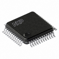
SC68C652BIB48,151 NXP Semiconductors, SC68C652BIB48,151 Datasheet - Page 41

SC68C652BIB48,151
Manufacturer Part Number
SC68C652BIB48,151
Description
IC UART DUAL W/FIFO 48-LQFP
Manufacturer
NXP Semiconductors
Datasheet
1.SC68C652BIB48151.pdf
(43 pages)
Specifications of SC68C652BIB48,151
Features
2 Channels
Number Of Channels
2, DUART
Fifo's
32 Byte
Voltage - Supply
2.5V, 3.3V, 5V
With Auto Flow Control
Yes
With Irda Encoder/decoder
Yes
With False Start Bit Detection
Yes
With Modem Control
Yes
Mounting Type
Surface Mount
Package / Case
48-LQFP
Transmitter And Receiver Fifo Counter
Yes
Data Rate
5Mbps
Package Type
LQFP
Operating Supply Voltage (max)
5.5V
Mounting
Surface Mount
Pin Count
48
Operating Temperature (min)
-40C
Operating Temperature (max)
85C
Operating Temperature Classification
Industrial
Lead Free Status / RoHS Status
Lead free / RoHS Compliant
Other names
568-3297
935278766151
SC68C652BIB48-S
935278766151
SC68C652BIB48-S
Available stocks
Company
Part Number
Manufacturer
Quantity
Price
Company:
Part Number:
SC68C652BIB48,151
Manufacturer:
NXP Semiconductors
Quantity:
10 000
NXP Semiconductors
14. Revision history
Table 33.
SC68C652B_2
Product data sheet
Document ID
SC68C652B_2
Modifications:
SC68C652B_1
(9397 750 14657)
Revision history
Release date
20091102
20050425
•
•
•
•
•
•
•
•
•
•
•
The format of this data sheet has been redesigned to comply with the new identity guidelines of
NXP Semiconductors.
Legal texts have been adapted to the new company name where appropriate.
Data sheet title modified from “... and Motorola P interface” to “... and 68 mode P interface”
Section 2
Table 10 “Interrupt Enable Register bits
68C450 mode” to “In the 16C450 mode”
Table 11 “FIFO Control Register bits
68C450 mode” to “in the 16C450 mode” (in 2 places)
Table 27 “Limiting
– Symbol V
– Symbol “P
– Parameter for T
Table 28 “Static
– Descriptive line below table title changed from “V
– Symbol/parameter changed from “V
– Symbol/parameter changed from “V
– Symbol changed from “I
– Parameter for I
Table 29 “Dynamic
– Descriptive line below table title changed from “V
– Symbol/parameter “t
–
– added
Figure 8 “External clock
– “t
– “t
– “t
Updated soldering information
“operating” moved to Conditions column
“tolerance of V
LOW-level input voltage”
HIGH-level input voltage”
“tolerance of V
“t
Table note
WL
w2
w1
w3
” changed to “t
” changed to “t
” changed to “t
, pulse width LOW”
“Features”, 3
Table note [4]
n
tot(pack)
[3]: denominator in equation changed from “t
split to show 2 separate conditions: “at D7 to D0 pins” and “at input only pins”
Data sheet status
Product data sheet
Product data sheet
characteristics”:
CC
CC
CC(sleep)
values”:
amb
characteristics”:
” changed to “P
Rev. 02 — 2 November 2009
WL
WH
w(clk)
rd
changed from “operating temperature” to “ambient temperature”;
10 %”
10 %”
1w
”
”
and its reference at t
timing”:
bullet item re-written; added
”
, t
changed from “sleep current” to “sleep mode supply current”
CL
2w
Dual UART with 32-byte FIFOs and IrDA encoder/decoder
” to “I
, clock cycle period” is split into “t
L(clk)
tot
description”, description of bit 3: changed from “in the
/pack”
”
IL(CK)
IH(CK)
description”, description of bit 0: changed from “In the
, LOW-level clock input voltage” to “V
, HIGH-level clock input voltage” to “V
(RESET)
Change notice
-
-
CC
CC
Footnote 1
= 2.5 V, 3.3 V
= 2.5 V, 3.3 V
3w
” to “t
WH
, pulse width HIGH” and
w(clk)
SC68C652B
Supersedes
SC68C652B_1
-
”
10 % or 5 V
10 % or 5 V
© NXP B.V. 2009. All rights reserved.
IL(clk)
IH(clk)
10 %” to
, clock
10 %” to
, clock
41 of 43


