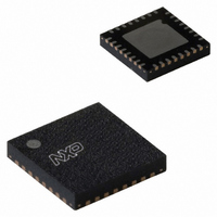
SC16C2550BIBS,157 NXP Semiconductors, SC16C2550BIBS,157 Datasheet - Page 8

SC16C2550BIBS,157
Manufacturer Part Number
SC16C2550BIBS,157
Description
IC DUART SOT617-1
Manufacturer
NXP Semiconductors
Datasheet
1.SC16C2550BIA44518.pdf
(43 pages)
Specifications of SC16C2550BIBS,157
Features
False-start Bit Detection
Number Of Channels
2, DUART
Fifo's
16 Byte
Voltage - Supply
3.5 V ~ 4.5 V
With Auto Flow Control
Yes
With False Start Bit Detection
Yes
With Modem Control
Yes
With Cmos
Yes
Mounting Type
Surface Mount
Package / Case
32-VFQFN Exposed Pad
Lead Free Status / RoHS Status
Lead free / RoHS Compliant
Other names
935280309157
SC16C2550BIBS
SC16C2550BIBS
SC16C2550BIBS
SC16C2550BIBS
NXP Semiconductors
Table 3.
SC16C2550B_5
Product data sheet
Symbol
DSRA
DSRB
DTRA
DTRB
RIA
RIB
RTSA
RTSB
RXA
RXB
TXA
TXB
n.c.
Pin
HVQFN32 DIP40 PLCC44 LQFP48
-
-
-
-
-
-
23
15
4
3
5
6
-
Pin description
37
22
33
34
39
23
32
24
10
9
11
12
-
…continued
41
25
37
38
43
26
36
27
11
10
13
14
-
39
20
34
35
41
21
33
22
5
4
7
8
12, 24,
25, 37
5 V, 3.3 V and 2.5 V dual UART, 5 Mbit/s (max.), with 16-byte FIFOs
Rev. 05 — 12 January 2009
Type
I
I
O
O
I
I
O
O
I
I
O
O
-
Description
Data Set Ready (active LOW). These inputs are associated
with individual UART channels, A through B. A logic 0 on this
pin indicates the modem or data set is powered-on and is ready
for data exchange with the UART. This pin has no effect on the
UART’s transmit or receive operation.
Data Terminal Ready (active LOW). These outputs are
associated with individual UART channels, A through B.
A logic 0 on this pin indicates that the SC16C2550B is
powered-on and ready. This pin can be controlled via the
Modem Control Register. Writing a logic 1 to MCR[0] will set
the DTRn output to logic 0, enabling the modem. This pin will
be a logic 1 after writing a logic 0 to MCR[0] or after a reset.
This pin has no effect on the UART’s transmit or receive
operation.
Ring Indicator (active LOW). These inputs are associated
with individual UART channels, A through B. A logic 0 on this
pin indicates the modem has received a ringing signal from the
telephone line. A logic 1 transition on this input pin will generate
an interrupt.
Request to Send (active LOW). These outputs are associated
with individual UART channels, A through B. A logic 0 on the
RTSn pin indicates the transmitter has data ready and waiting
to send. Writing a logic 1 in the Modem Control Register
MCR[1] will set this pin to a logic 0, indicating data is available.
After a reset this pin will be set to a logic 1. This pin has no
effect on the UART’s transmit or receive operation.
Receive data A, B. These inputs are associated with individual
serial channel data to the SC16C2550B receive input circuits,
A and B. The RXn signal will be a logic 1 during reset, idle (no
data) or when the transmitter is disabled. During the local
Loopback mode, the RXn input pin is disabled and TX data is
connected to the UART RX input, internally.
Transmit data A, B. These outputs are associated with
individual serial transmit channel data from the SC16C2550B.
The TXn signal will be a logic 1 during reset, idle (no data) or
when the transmitter is disabled. During the local Loopback
mode, the TXn output pin is disabled and TX data is internally
connected to the UART RX input.
not connected
SC16C2550B
© NXP B.V. 2009. All rights reserved.
8 of 43


