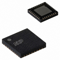
SC16C852LIBS,151 NXP Semiconductors, SC16C852LIBS,151 Datasheet - Page 8

SC16C852LIBS,151
Manufacturer Part Number
SC16C852LIBS,151
Description
IC UART DUAL W/FIFO 32-HVQFN
Manufacturer
NXP Semiconductors
Type
IrDA or RS- 485r
Datasheet
1.SC16C852LIBS151.pdf
(64 pages)
Specifications of SC16C852LIBS,151
Number Of Channels
2, DUART
Package / Case
32-VFQFN Exposed Pad
Features
Programmable
Fifo's
128 Byte
Protocol
RS485
Voltage - Supply
1.8V
With Auto Flow Control
Yes
With Irda Encoder/decoder
Yes
With False Start Bit Detection
Yes
With Modem Control
Yes
With Cmos
Yes
Mounting Type
Surface Mount
Data Rate
5 Mbps
Supply Voltage (max)
1.95 V
Supply Voltage (min)
1.65 V
Supply Current
5 mA
Maximum Operating Temperature
+ 85 C
Minimum Operating Temperature
- 40 C
Mounting Style
SMD/SMT
Operating Supply Voltage
1.8 V
Transmitter And Receiver Fifo Counter
Yes
Mounting
Surface Mount
Pin Count
32
Operating Temperature (min)
-40C
Operating Temperature (max)
85C
Operating Temperature Classification
Industrial
Lead Free Status / RoHS Status
Lead free / RoHS Compliant
Lead Free Status / RoHS Status
Lead free / RoHS Compliant, Lead free / RoHS Compliant
Other names
568-4209
935283101151
SC16C852LIBS-S
935283101151
SC16C852LIBS-S
NXP Semiconductors
Table 2.
SC16C852L
Product data sheet
Symbol
A0
A1
A2
CDA
CDB
CSA/CS
CSB/A3
CTSA
CTSB
DSRA
DSRB
DTRA
DTRB
D0
D1
D2
D3
D4
D5
D6
D7
Pin description
11
Pin
LQFP48
28
27
26
40
16
10
38
23
39
20
34
35
44
45
46
47
48
1
2
3
5.2 Pin description
HVQFN32 TFBGA36
20
19
18
-
-
7
8
25
16
-
-
-
-
27
28
29
30
31
32
1
2
D5
D6
E6
-
-
E2
F1
A5
E5
-
-
-
-
A3
B3
A2
B2
A1
B1
C3
C1
All information provided in this document is subject to legal disclaimers.
1.8 V dual UART with 128-byte FIFOs and IrDA encoder/decoder
Type
I
I
I
I
I
I
I
I
I
I
O
I/O
I/O
I/O
I/O
I/O
I/O
I/O
I/O
Rev. 4 — 1 February 2011
Description
Address 0 select bit. Internal register address selection.
Address 1 select bit. Internal register address selection.
Address 2 select bit. Internal register address selection.
Carrier Detect (active LOW). These inputs are associated with
individual UART channels A through B. A logic 0 on this pin
indicates that a carrier has been detected by the modem for that
channel.
When 16/68 pin is at logic 1 (or unconnected), this input is chip
select for channel A.
When 16/68 pin is at logic 0, this input becomes the chip select for
both channels (Motorola mode).
When 16/68 pin is at logic 1 (or unconnected), this input is chip
select for channel B.
When 16/68 pin is at logic 0, this input becomes the address line
A3 which is used for channel selection; a logic 0 selects channel A
and a logic 1 selects channel B.
Clear to Send (active LOW). These inputs are associated with
individual UART channels, A through B. A logic 0 on the CTSx pin
indicates the modem or data set is ready to accept transmit data
from the SC16C852L. Status can be tested by reading MSR[4].
Data Set Ready (active LOW). These inputs are associated with
individual UART channels, A through B. A logic 0 on this pin
indicates the modem or data set is powered-on and is ready for
data exchange with the UART. Status can be tested by reading
MSR[5].
Data Terminal Ready (active LOW). These outputs are
associated with individual UART channels, A through B. A logic 0
on this pin indicates that the SC16C852L is powered-on and ready.
This pin can be controlled via the modem control register. Writing a
logic 1 to MCR[0] will set the DTRx output to logic 0, enabling the
modem. This pin will be a logic 1 after writing a logic 0 to MCR[0],
or after a reset.
Data bus (bidirectional). These pins are the 8-bit, 3-state data
bus for transferring information to or from the controlling CPU. D0
is the least significant bit and the first data bit in a transmit or
receive serial data stream.
SC16C852L
© NXP B.V. 2011. All rights reserved.
8 of 64


