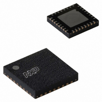
SC16C852LIBS,151 NXP Semiconductors, SC16C852LIBS,151 Datasheet - Page 19

SC16C852LIBS,151
Manufacturer Part Number
SC16C852LIBS,151
Description
IC UART DUAL W/FIFO 32-HVQFN
Manufacturer
NXP Semiconductors
Type
IrDA or RS- 485r
Datasheet
1.SC16C852LIBS151.pdf
(64 pages)
Specifications of SC16C852LIBS,151
Number Of Channels
2, DUART
Package / Case
32-VFQFN Exposed Pad
Features
Programmable
Fifo's
128 Byte
Protocol
RS485
Voltage - Supply
1.8V
With Auto Flow Control
Yes
With Irda Encoder/decoder
Yes
With False Start Bit Detection
Yes
With Modem Control
Yes
With Cmos
Yes
Mounting Type
Surface Mount
Data Rate
5 Mbps
Supply Voltage (max)
1.95 V
Supply Voltage (min)
1.65 V
Supply Current
5 mA
Maximum Operating Temperature
+ 85 C
Minimum Operating Temperature
- 40 C
Mounting Style
SMD/SMT
Operating Supply Voltage
1.8 V
Transmitter And Receiver Fifo Counter
Yes
Mounting
Surface Mount
Pin Count
32
Operating Temperature (min)
-40C
Operating Temperature (max)
85C
Operating Temperature Classification
Industrial
Lead Free Status / RoHS Status
Lead free / RoHS Compliant
Lead Free Status / RoHS Status
Lead free / RoHS Compliant, Lead free / RoHS Compliant
Other names
568-4209
935283101151
SC16C852LIBS-S
935283101151
SC16C852LIBS-S
NXP Semiconductors
SC16C852L
Product data sheet
6.10 DMA operation
6.11 Loopback mode
The SC16C852L FIFO trigger level provides additional flexibility to the user for block
mode operation. The user can optionally operate the transmit and receive FIFOs in the
DMA mode (FCR[3]). The DMA mode affects the state of the RXRDYA/RXRDYB and
TXRDYA/TXRDYB output pins.
Table 8.
[1]
Table 9.
[1]
The internal loopback capability allows on-board diagnostics. In the Loopback mode, the
normal modem interface pins are disconnected and reconfigured for loopback internally
(see
testing. In the Loopback mode, the transmitter output (TX) and the receiver input (RX) are
disconnected from their associated interface pins, and instead are connected together
internally. The CTS, DSR, CD, and RI are disconnected from their normal modem control
input pins, and instead are connected internally to RTS, DTR, MCR[3] (OP2A/OP2B) and
MCR[2] (OP1A/OP1B). Loopback test data is entered into the transmit holding register via
the user data bus interface, D[7:0]. The transmit UART serializes the data and passes the
serial data to the receive UART via the internal loopback connection. The receive UART
converts the serial data back into parallel data that is then made available at the user data
interface D[7:0]. The user optionally compares the received data to the initial transmitted
data for verifying error-free operation of the UART TX/RX circuits.
In this mode, the interrupt pin is 3-stated, therefore, the software must use the polling
method (see
Non-DMA mode
Non-DMA mode
0 = FIFO empty
1 = FIFO empty
0 = at least 1 byte in FIFO
1 = at least 1 byte in FIFO
Receive FIFO becomes full at 32 bytes when in normal mode. When TXINTLVL or RXINTLVL or FLWCNTH
or FLWCNTL contains any value other than 0x00 (extended mode), then the receive FIFO becomes full at
128 bytes.
Transmit FIFO becomes full at 32 bytes when in normal mode. When TXINTLVL or RXINTLVL or
FLWCNTH or FLWCNTL contains any value other than 0x00 (extended mode), then the transmit FIFO
becomes full at 128 bytes.
Figure
Effect of DMA mode on state of RXRDYA/RXRDYB pin
Effect of DMA mode on state of TXRDYA/TXRDYB pin
10). MCR[3:0] register bits are used for controlling loopback diagnostic
Section
All information provided in this document is subject to legal disclaimers.
1.8 V dual UART with 128-byte FIFOs and IrDA encoder/decoder
7.2.2) to send and receive data.
Rev. 4 — 1 February 2011
0-to-1 transition when FIFO empties
1-to-0 transition when FIFO has at least one empty location
DMA mode
1-to-0 transition when FIFO reaches trigger level, or time-out
occurs
DMA mode
0-to-1 transition when FIFO becomes full
Table 8
[1]
and
Table 9
show this.
[1]
SC16C852L
© NXP B.V. 2011. All rights reserved.
19 of 64


