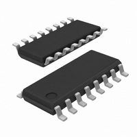
SI3200-FS Silicon Laboratories Inc, SI3200-FS Datasheet - Page 39

SI3200-FS
Manufacturer Part Number
SI3200-FS
Description
IC LINEFEED INTRFC 100V 16SOIC
Manufacturer
Silicon Laboratories Inc
Series
ProSLIC®r
Specifications of SI3200-FS
Package / Case
16-SOIC (3.9mm Width)
Function
Subscriber Line Interface Concept (SLIC), CODEC
Interface
GCI, PCM, SPI
Number Of Circuits
2
Voltage - Supply
3.3V, 5V
Current - Supply
110µA
Power (watts)
941mW
Operating Temperature
-40°C ~ 85°C
Mounting Type
Surface Mount
Includes
Battery Switching, BORSCHT Functions, DTMF Generation and Decoding, FSK Tone Generation, Modem and Fax Tone Detection
Product
SLIC
Supply Voltage (min)
3.13 V
Supply Current
0.11 mA, 8.8 mA
Maximum Operating Temperature
+ 70 C
Minimum Operating Temperature
0 C
Mounting Style
SMD/SMT
Number Of Channels
2
Lead Free Status / RoHS Status
Lead free / RoHS Compliant
Available stocks
Company
Part Number
Manufacturer
Quantity
Price
Part Number:
SI3200-FS
Manufacturer:
SILICON LABS/芯科
Quantity:
20 000
Company:
Part Number:
SI3200-FSR
Manufacturer:
SILICON
Quantity:
11 430
Power Dissipation Considerations
The Dual ProSLIC devices rely on the Si3200 to power
the line from the battery supply. The PCB layout and
enclosure conditions should be designed to allow
sufficient thermal dissipation out of the Si3200, and a
programmable power alarm threshold ensures product
safety under all operating conditions. See "Power
Monitoring and Power Fault Detection" on page 35 for
more details on power alarm considerations.
The Si3200’s thermally-enhanced SOIC-16 package
offers an exposed pad that improves thermal dissipation
out of the package when soldered to a topside PCB pad
connected to inner power planes. Using appropriate
layout practices, the Si3200 can provide thermal
performance of 55 °C/W. The exposed path should be
connected to a low-impedance ground plane via a
topside PCB pad directly under the part. See package
outlines for PCB pad dimensions. In addition, an
opposite-side PCB pad with multiple vias connecting it
to the topside pad directly under the exposed pad will
further improve the overall thermal performance of the
system. Refer to “AN55: Dual ProSLIC User Guide” for
optimal thermal dissipation layout guidelines.
The Dual ProSLIC chipset is designed with the ability to
source long loop lengths in excess of 18 kft but can also
accommodate short loop configurations. For example,
the Si3220 can operate from one of two battery supplies
depending on the operating state. When in the on-hook
Parameter
Si3200 Total Power Output Monitor
Si3200 Power Alarm Interrupt Pending
Si3200 Power Alarm Interrupt Enable
Q1/Q2 Power Alarm Threshold (discrete)
Q1/Q2 Power Alarm Threshold (Si3200)
Q3/Q4 Power Alarm Threshold
Q5/Q6 Power Alarm Threshold
Q1/Q2 Thermal LPF Pole
Q3/Q4 Thermal LPF Pole
Q5/Q6 Thermal LPF Pole
Q1–Q6 Power Alarm Interrupt Pending
Q1–Q6 Power Alarm Interrupt Enable
Table 21. Register and RAM Locations Used for Power Monitoring and Power Fault Detection
Mnemonic
IRQVEC3
IRQVEC3
Register/
IRQEN3
IRQEN3
PLPF12
PLPF34
PLPF56
PTH12
PTH34
PTH56
PSUM
RAM
Rev. 1.0
state, the on-hook loop feed is generated from the
ringing battery supply, generally –70 V or more. Once
the SLIC transitions to the off-hook state, a lower off-
hook battery supply (typically –24 V) supplies the
required current to power the loop if the loop length is
sufficiently short to accommodate the lower battery
supply. This battery switching method allows the SLIC
chipset to dissipate less power than when operating
from a –70 V battery supply. See “Automatic Dual
Battery Switching” for more details.
In long loop applications, there is generally a single
battery supply (e.g., –48 V) available for powering the
loop in the off-hook state. When sourcing loop lengths
similar to the maximum specified service distance (e.g.,
18 kft.), most of the power is dissipated in the
impedance of the line. SLICs used in long-loop
applications must also be able to provide phone service
to customers who are located much closer to the line
card than the maximum loop length specified for the
system. This situation may cause substantial power to
be dissipated inside the SLIC chipset, often resulting in
thermal shutdown or destruction of the device due to
thermal runaway. A special power offload circuit is
recommended
applications. Refer to “AN91: Si3200 Power Off-load
Circuit” for power offload circuit usage guidelines.
Register/RAM
PLPF12[15:3]
PLPF34[15:3]
PLPF56[15:3]
PQ1S–PQ6S
PQ1E–PQ6E
PTH12[15:0]
PTH34[15:0]
PTH56[15:0]
PSUM[15:0]
PQ1S
PQ1E
Bits
for
Measurement
See “Power Filter and Alarms”
See “Power Filter and Alarms”
See “Power Filter and Alarms”
0 to 16.319 W
0 to 16.319 W
Si3220/Si3225
0 to 34.72 W
0 to 34.72 W
0 to 1.03 W
single-battery
Range
N/A
N/A
N/A
N/A
extended-loop
Resolution
1059.6 µ W
1059.6 µ W
31.4 µ W
498 µ W
498 µ W
N/A
N/A
N/A
N/A
39


