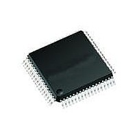
MAX2991ECM+ Maxim Integrated Products, MAX2991ECM+ Datasheet - Page 12

MAX2991ECM+
Manufacturer Part Number
MAX2991ECM+
Description
IC TXRX FRONT-END 48LQFP
Manufacturer
Maxim Integrated Products
Type
General Purposer
Datasheet
1.MAX2991ECM.pdf
(22 pages)
Specifications of MAX2991ECM+
Function
Analog Front-End Transceiver
Interface
SPI Serial
Number Of Circuits
1
Voltage - Supply
3 V ~ 3.6 V
Current - Supply
36mA, 70mA
Power (watts)
1.54W
Operating Temperature
-40°C ~ 85°C
Mounting Type
Surface Mount
Package / Case
48-LQFP
Includes
Automatic Gain Control (AGC)
Product
Analog Front End
Data Rate
1.2 Msps
Interface Type
Digital
Supply Voltage (max)
3.6 V
Supply Voltage (min)
3 V
Supply Current
36 mA, 70 mA
Maximum Operating Temperature
+ 85 C
Minimum Operating Temperature
- 40 C
Maximum Power Dissipation
1535 mW
Mounting Style
SMD/SMT
Number Of Channels
2
Lead Free Status / RoHS Status
Lead free / RoHS Compliant
Table 1 shows the MAX2991 register map.
Table 1. Register Map
Power-Line Communications (PLC) Integrated
Analog Front-End Transceiver
The AGCCS signal controls the AGC circuit of the receive
path in the MAX2991. A logic-low on AGCCS sets the
gain circuit on the input signal to continuously adapt for
maximum sensitivity. A valid preamble detected by the
digital PHY raises AGCCS to high. While AGCCS is high,
the AGC continues to adapt for an additional program-
mable delay, then the AGC locks the currently adapted
level on the incoming signal. The digital PHY holds
AGCCS high while receiving a transmission and then
lowers AGCCS for continuous adaptation for maximum
sensitivity of other incoming signals.
Use the AGCFRZ signal to instantly lock the VGA1 and
VGA2 gains.
The RST signal provides reset control for the MAX2991.
Drive RST low to place the MAX2991 in reset mode.
Leave Rx and Tx clocks in free-running mode during a
reset. The minimum reset pulse width is 100ns.
The MAX2991 features four power-down modes:
1) Global Power-Down Mode: Enter this mode either
12
REGISTER
by setting the SHDN input to logic-low or by setting
the CHIPENB bit (bit 0 of RXCONF register) to 1. All
clocks to the digital circuitry are gated. Set SHDN to
IIR0CONF
RXCONF
TXCONF
PTUN1
PTUN2
_____________________________________________________________________________________
IIR0B0
IIR0B1
AGC3
—
—
—
—
—
—
—
WIDTH
<13:0>
<15:0>
<13:0>
<13:0>
<11:0>
<11:0>
<13:0>
<13:0>
<14:0>
<15:0>
<15:0>
<15:0>
<5:0>
<9:0>
<8:0>
AGC Control Signals (AGCCS)
AGC Freeze Mode (AGCFRZ)
ADDRESS
Power-Down Modes
0x0A
0x0B
0x0C
0x0D
0x00
0x01
0x02
0x03
0x04
0x05
0x06
0x07
0x08
0x09
0x0E
Reset Input (RST)
Rx configuration and control
Tx configuration and control
Reserved
Process tuner configuration and control
Process tuner manual override
Reserved
Reserved
AGC configuration and control
Reserved
Reserved
Reserved
Reserved
IIR filter configuration of first biquad
IIR filter B0 coefficient of first biquad
IIR filter B1 coefficient of first biquad
2) Idle Mode: Enter this mode by setting the IDLEEN
3) Transmit Power-Down Mode: Enter this mode by
4) Receive Power-Down Mode: Enter this mode by set-
logic-high or set the CHIPENB bit to logic-low to exit
this mode. The Tx and Rx blocks are fully operational
approximately 20Fs after coming out of global power-
down mode.
bit to 1. In this mode, all blocks are powered down
except for the AFE interface and the bias blocks.
RXCLK and TXCLK are not gated. Set IDLEEN to 0 to
exit this mode. The Tx and Rx blocks are fully opera-
tional approximately 20Fs after coming out of global
power-down mode.
setting ENTX to logic-high while the ENTXBEN bit
(bit 0 of register TXCONF) is set to 1. In this mode,
the transmit predriver, lowpass filter, and the DAC
are powered down. Set ENTX to logic-low to exit this
mode. The Tx block is fully operational approximately
15Fs after coming out of global power-down mode.
ting ENRX to logic-high while the ENRXBEN bit (bit
2 of register RXCONF) is set to 1. In this mode, the
receiver VGA1, VGA2, lowpass filter, lowpass filter
buffer, highpass filter, and the ADC are powered
down. Set ENRX to logic-low to exit this mode. The
Rx block is fully operational approximately 20Fs after
coming out of global power-down mode.
FUNCTION
Register Map
DEFAULT
0x0825C
0x282B
0xF43A
0x0004
0x0000
0x0320
0x0000
0x0200
0x0000
0xE8E
0x0ED
0x000
0xE00
0x000
0x13


