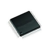
MAX2991ECM+ Maxim Integrated Products, MAX2991ECM+ Datasheet - Page 11

MAX2991ECM+
Manufacturer Part Number
MAX2991ECM+
Description
IC TXRX FRONT-END 48LQFP
Manufacturer
Maxim Integrated Products
Type
General Purposer
Datasheet
1.MAX2991ECM.pdf
(22 pages)
Specifications of MAX2991ECM+
Function
Analog Front-End Transceiver
Interface
SPI Serial
Number Of Circuits
1
Voltage - Supply
3 V ~ 3.6 V
Current - Supply
36mA, 70mA
Power (watts)
1.54W
Operating Temperature
-40°C ~ 85°C
Mounting Type
Surface Mount
Package / Case
48-LQFP
Includes
Automatic Gain Control (AGC)
Product
Analog Front End
Data Rate
1.2 Msps
Interface Type
Digital
Supply Voltage (max)
3.6 V
Supply Voltage (min)
3 V
Supply Current
36 mA, 70 mA
Maximum Operating Temperature
+ 85 C
Minimum Operating Temperature
- 40 C
Maximum Power Dissipation
1535 mW
Mounting Style
SMD/SMT
Number Of Channels
2
Lead Free Status / RoHS Status
Lead free / RoHS Compliant
The MAX2991 power-line AFE integrated circuit is a
state-of-the-art CMOS device that delivers high perfor-
mance and low cost. This highly integrated design com-
bines an ADC, DAC, signal conditioning, and predriver
as shown in the Functional Diagram. The MAX2991
meets all frequency band requirements of the various
popular power-line standards such as FCC, ARIB, and
CENELEC.
The MAX2991 along with the MAX2990 PLC baseband
modem deliver the most cost-effective data communi-
cation solution over power-line networks in the market.
The advanced design of the MAX2991 allows operation
without external controls, enabling simplified connection
to a variety of third-party power-line digital PHY devices.
The MAX2991 includes various control signals to achieve
additional power reduction.
The receiver channel consists of a low-noise variable-
gain amplifier (VGA1) followed by a lowpass filter (LPF),
a highpass filter (HPF), and another variable-gain ampli-
fier (VGA2) circuit. An ADC samples the VGA2 output.
An AFE interface provides data communication to the
digital PHY device.
The variable-gain low-noise amplifier reduces the receiv-
er channel input-referred noise by providing additional
signal gain to the AFE input. The filter blocks remove
any out-of-band noise, provide anti-aliasing, and select a
proper AFE bandwidth. Using the adaptation blocks, the
VGAs scale the received signal to maintain the optimum
signal level at the ADC input.
The 10-bit ADC samples the analog signal and converts
it to a 10-bit digital stream with a maximum 1.2Msps
sampling rate.
The transmit channel consists of a 10-bit DAC, an image-
reject lowpass filter, and a programmable-gain predriv-
er. The DAC receives the data stream from the digital
PHY device through the AFE interface. The 10-bit DAC
provides a complementary function to the receive chan-
nel with a maximum 1.2Msps sampling rate. The DAC
converts the 10-bit digital stream to an analog voltage.
The lowpass filter removes spurs and harmonics adja-
cent to the desired passband to reduce any out-of-band
transmitted frequencies and energy from the DAC out-
put. The lowpass filter ensures that the transmitted signal
Power-Line Communications (PLC) Integrated
______________________________________________________________________________________
Detailed Description
Transmit Channel
Receive Channel
Analog Front-End Transceiver
meets bandwidth requirements specified by the different
wideband and narrowband standards.
The predriver controls the output level of the lowpass
filter connected to an external line driver, which, in turn,
connects to the power-line medium. The output level is
adjustable by the predriver gain control that provides up
to 6dB gain and 10dB attenuation.
The MAX2991 features two separate serial interfaces:
host SPI interface and AFE interface. The host SPI inter-
face provides direct access to the MAX2991 configura-
tion registers, while the AFE interface allows data com-
munication with the PLC baseband modem (MAX2990)
and also provides indirect access to the MAX2991 con-
figuration registers.
The MAX2991 host SPI interface provides access to
the configuration registers using CS, SCLK, SDIN, and
SDOUT. A host SPI frame consists of a 7-bit register
address, a read/write bit, and 16 bits of data. Data is
driven on the rising edge of SCLK and sampled on the
falling edge of SCLK. Figure 3 shows a valid host SPI
communication protocol.
The AFE interface allows the MAX2991 to communicate
with the PLC baseband modem (MAX2990) through
a transmit channel (TXCLK, TXDATA, TXCONV) and
a receive channel (RXCLK, RXDATA, RXCONV), and
provides indirect access to the MAX2991 configuration
registers. See the Interfacing to the MAX2990 Baseband
section for connection details.
ENTX enables the transmitter of the MAX2991 AFE cir-
cuit. A logic-high on ENTX powers down the MAX2991
transmitter.
ENRX enables the receiver on the MAX2991. A logic-
high on ENRX powers down the MAX2991 receiver.
The TXCLK signal provides the clock to the MAX2991
AFE transmitter. Apply a 19.2MHz clock at TXCLK to
achieve 1.2Msps data rate.
The RXCLK signal provides the clock to the MAX2991
AFE receiver. Apply a 19.2MHz clock at RXCLK to
achieve 1.2Msps data rate.
AFE Interface Receiver Enable (ENRX)
AFE Interface Transmit Enable (ENTX)
AFE Interface Rx Clock (RXCLK)
AFE Interface Tx Clock (TXCLK)
Serial Interface
Host SPI Interface
AFE Interface
11


