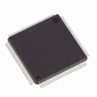
DS2155L+ Maxim Integrated Products, DS2155L+ Datasheet - Page 144

DS2155L+
Manufacturer Part Number
DS2155L+
Description
IC TXRX T1/E1/J1 1-CHIP 100-LQFP
Manufacturer
Maxim Integrated Products
Datasheet
1.DS2155L.pdf
(238 pages)
Specifications of DS2155L+
Function
Single-Chip Transceiver
Interface
E1, HDLC, J1, T1
Number Of Circuits
1
Voltage - Supply
3.14 V ~ 3.47 V
Current - Supply
75mA
Operating Temperature
0°C ~ 70°C
Mounting Type
Surface Mount
Package / Case
100-LQFP
Includes
BERT Generator and Detector, CMI Coder and Decoder, HDLC Controller
Product
Framer
Number Of Transceivers
1
Data Rate
64 Kbps
Supply Voltage (max)
3.465 V
Supply Voltage (min)
3.135 V
Supply Current (max)
75 mA (Typ)
Maximum Operating Temperature
+ 70 C
Minimum Operating Temperature
0 C
Mounting Style
SMD/SMT
Lead Free Status / RoHS Status
Lead free / RoHS Compliant
Power (watts)
-
Lead Free Status / Rohs Status
Lead free / RoHS Compliant
- Current page: 144 of 238
- Download datasheet (2Mb)
Normally, the clock that is output at the RCLK pin is the recovered clock from the E1 AMI/HDB3 or T1
AMI/B8ZS waveform presented at the RTIP and RRING inputs. If the jitter attenuator is placed in the
receive path (as is the case in most applications), the jitter attenuator restores the RCLK to an
approximate 50% duty cycle. If the jitter attenuator is either placed in the transmit path or is disabled, the
RCLK output can exhibit slightly shorter high cycles of the clock. This is because of the highly over-
sampled digital-clock recovery circuitry. See the Receive AC Timing Characteristics in Section
more details. When no signal is present at RTIP and RRING, a receive carrier loss (RCL) condition
occurs and the RCLK is derived from the JACLK source.
24.2.1 Receive Level Indicator and Threshold Interrupt
The DS2155 reports the signal strength at RTIP and RRING in 2.5dB increments through RL3–RL0
located in Information Register 2 (INFO2). This feature is helpful when trouble-shooting line-
performance problems. The DS2155 can initiate an interrupt whenever the input falls below a certain
level through the input-level under-threshold indicator (SR1.7). Using the RLT0–RLT4 bits of the CCR4
register, the user can set a threshold in 2.5dB increments. The SR1.7 bit is set whenever the input level at
RTIP and RRING falls below the threshold set by the value in RLT0–RLT4. The level must remain
below the programmed threshold for approximately 50ms for this bit to be set. The accuracy of the
receive level indication is +/- 1 LSB (2.5dB) from 25C to 85C and +/- 2 LSB’s (5dB) from –40C to 25C.
24.2.2 Receive G.703 Synchronization Signal (E1 Mode)
The DS2155 is capable of receiving a 2.048MHz square-wave synchronization clock as specified in
Section 13 of ITU G.703, October 1998. In order to use the DS2155 in this mode, set the receive
synchronization clock enable (LIC3.2) = 1.
24.2.3 Monitor Mode
Monitor applications in both E1 and T1 require various flat gain settings for the receive-side circuitry.
The DS2155 can be programmed to support these applications through the monitor mode control bits
MM1 and MM0 in the LIC3 register
Figure 24-1. Typical Monitor Application
T1/E1 LINE
Rm
MONITOR
PORT JACK
Rm
(Figure
PRIMARY
T1/E1 TERMINATING
DEVICE
24-1).
144 of 238
X
F
M
R
SECONDARY T1/E1
TERMINATING
DEVICE
Rt
DS2156
37.3
for
Related parts for DS2155L+
Image
Part Number
Description
Manufacturer
Datasheet
Request
R

Part Number:
Description:
Manufacturer:
Maxim Integrated Products
Datasheet:

Part Number:
Description:
Ds2155 T1/e1/j1 Single-chip Transceiver
Manufacturer:
Maxim Integrated Products, Inc.
Datasheet:

Part Number:
Description:
MAX7528KCWPMaxim Integrated Products [CMOS Dual 8-Bit Buffered Multiplying DACs]
Manufacturer:
Maxim Integrated Products
Datasheet:

Part Number:
Description:
Single +5V, fully integrated, 1.25Gbps laser diode driver.
Manufacturer:
Maxim Integrated Products
Datasheet:

Part Number:
Description:
Single +5V, fully integrated, 155Mbps laser diode driver.
Manufacturer:
Maxim Integrated Products
Datasheet:

Part Number:
Description:
VRD11/VRD10, K8 Rev F 2/3/4-Phase PWM Controllers with Integrated Dual MOSFET Drivers
Manufacturer:
Maxim Integrated Products
Datasheet:

Part Number:
Description:
Highly Integrated Level 2 SMBus Battery Chargers
Manufacturer:
Maxim Integrated Products
Datasheet:

Part Number:
Description:
Current Monitor and Accumulator with Integrated Sense Resistor; ; Temperature Range: -40°C to +85°C
Manufacturer:
Maxim Integrated Products

Part Number:
Description:
TSSOP 14/A°/RS-485 Transceivers with Integrated 100O/120O Termination Resis
Manufacturer:
Maxim Integrated Products

Part Number:
Description:
TSSOP 14/A°/RS-485 Transceivers with Integrated 100O/120O Termination Resis
Manufacturer:
Maxim Integrated Products

Part Number:
Description:
QFN 16/A°/AC-DC and DC-DC Peak-Current-Mode Converters with Integrated Step
Manufacturer:
Maxim Integrated Products

Part Number:
Description:
TDFN/A/65V, 1A, 600KHZ, SYNCHRONOUS STEP-DOWN REGULATOR WITH INTEGRATED SWI
Manufacturer:
Maxim Integrated Products

Part Number:
Description:
Integrated Temperature Controller f
Manufacturer:
Maxim Integrated Products

Part Number:
Description:
SOT23-6/I°/45MHz to 650MHz, Integrated IF VCOs with Differential Output
Manufacturer:
Maxim Integrated Products

Part Number:
Description:
SOT23-6/I°/45MHz to 650MHz, Integrated IF VCOs with Differential Output
Manufacturer:
Maxim Integrated Products


