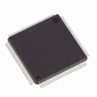
DS2155L+ Maxim Integrated Products, DS2155L+ Datasheet - Page 142

DS2155L+
Manufacturer Part Number
DS2155L+
Description
IC TXRX T1/E1/J1 1-CHIP 100-LQFP
Manufacturer
Maxim Integrated Products
Datasheet
1.DS2155L.pdf
(238 pages)
Specifications of DS2155L+
Function
Single-Chip Transceiver
Interface
E1, HDLC, J1, T1
Number Of Circuits
1
Voltage - Supply
3.14 V ~ 3.47 V
Current - Supply
75mA
Operating Temperature
0°C ~ 70°C
Mounting Type
Surface Mount
Package / Case
100-LQFP
Includes
BERT Generator and Detector, CMI Coder and Decoder, HDLC Controller
Product
Framer
Number Of Transceivers
1
Data Rate
64 Kbps
Supply Voltage (max)
3.465 V
Supply Voltage (min)
3.135 V
Supply Current (max)
75 mA (Typ)
Maximum Operating Temperature
+ 70 C
Minimum Operating Temperature
0 C
Mounting Style
SMD/SMT
Lead Free Status / RoHS Status
Lead free / RoHS Compliant
Power (watts)
-
Lead Free Status / Rohs Status
Lead free / RoHS Compliant
- Current page: 142 of 238
- Download datasheet (2Mb)
23.5.3 Transmit Section
The transmit section shifts out into the T1 data stream either the FDL (in the ESF framing mode) or the
Fs bits (in the D4 framing mode) contained in the transmit FDL register (TFDL). When a new value is
written to the TFDL, it is multiplexed serially (LSB first) into the proper position in the outgoing T1 data
stream. After the full 8 bits have been shifted out, the framer signals the host microcontroller by setting
the SR8.2 bit to a 1 that the buffer is empty and that more data is needed. The INT also toggles low if
enabled through IMR8.2. The user has 2ms to update the TFDL with a new value. If the TFDL is not
updated, the old value in the TFDL is transmitted once again. The framer also contains a zero stuffer that
is controlled through the T1TCR2.5 bit. In both ANSI T1.403 and TR54016, communications on the FDL
follows a subset of an LAPD protocol. The LAPD protocol states that no more than five 1s should be
transmitted in a row so that the data does not resemble an opening or closing flag (01111110) or an abort
signal (11111111). If enabled through T1TCR2.5, the framer automatically looks for five 1s in a row. If it
finds such a pattern, it automatically inserts a 0 after the five 1s. The T1TCR2.5 bit should always be set
to a 1 when the framer is inserting the FDL.
Register Name:
Register Description:
Register Address:
Bit #
Name
Default
Note: Also used to insert Fs framing pattern in D4 framing mode.
The transmit FDL register (TFDL) contains the FDL information that is to be inserted on a byte basis into the
outgoing T1 data stream. The LSB is transmitted first.
Bit 0/Transmit FDL Bit 0 (TFDL0). LSB of the transmit FDL code.
Bit 1/Transmit FDL Bit 1 (TFDL1)
Bit 2/Transmit FDL Bit 2 (TFDL2)
Bit 3/Transmit FDL Bit 3 (TFDL3)
Bit 4/Transmit FDL Bit 4 (TFDL4)
Bit 5/Transmit FDL Bit 5 (TFDL5)
Bit 6/Transmit FDL Bit 6 (TFDL6)
Bit 7/Transmit FDL Bit 7 (TFDL7). MSB of the transmit FDL code.
23.6 D4/SLC-96 Operation
In the D4 framing mode, the framer uses the TFDL register to insert the Fs framing pattern. To allow the
device to properly insert the Fs framing pattern, the TFDL register at address C1h must be programmed to
1Ch and the following bits must be programmed as shown:
Since the SLC-96 message fields share the Fs-bit position, the user can access these message fields
through the TFDL and RFDL registers. Refer to Application Note 345: DS2141A, DS2151, DS2152 SLC-
96 for a detailed description about implementing an SLC-96 function.
TFDL7
7
0
T1TCR2.6 = 1 (allow the TFDL register to load on multiframe boundaries)
TFDL6
TFDL
Transmit FDL Register
C1h
6
0
T1TCR1.2 = 0 (source Fs data from the TFDL register)
TFDL5
5
0
TFDL4
4
0
142 of 238
TFDL3
3
0
TFDL2
2
0
TFDL1
1
0
TFDL0
0
0
Related parts for DS2155L+
Image
Part Number
Description
Manufacturer
Datasheet
Request
R

Part Number:
Description:
Manufacturer:
Maxim Integrated Products
Datasheet:

Part Number:
Description:
Ds2155 T1/e1/j1 Single-chip Transceiver
Manufacturer:
Maxim Integrated Products, Inc.
Datasheet:

Part Number:
Description:
MAX7528KCWPMaxim Integrated Products [CMOS Dual 8-Bit Buffered Multiplying DACs]
Manufacturer:
Maxim Integrated Products
Datasheet:

Part Number:
Description:
Single +5V, fully integrated, 1.25Gbps laser diode driver.
Manufacturer:
Maxim Integrated Products
Datasheet:

Part Number:
Description:
Single +5V, fully integrated, 155Mbps laser diode driver.
Manufacturer:
Maxim Integrated Products
Datasheet:

Part Number:
Description:
VRD11/VRD10, K8 Rev F 2/3/4-Phase PWM Controllers with Integrated Dual MOSFET Drivers
Manufacturer:
Maxim Integrated Products
Datasheet:

Part Number:
Description:
Highly Integrated Level 2 SMBus Battery Chargers
Manufacturer:
Maxim Integrated Products
Datasheet:

Part Number:
Description:
Current Monitor and Accumulator with Integrated Sense Resistor; ; Temperature Range: -40°C to +85°C
Manufacturer:
Maxim Integrated Products

Part Number:
Description:
TSSOP 14/A°/RS-485 Transceivers with Integrated 100O/120O Termination Resis
Manufacturer:
Maxim Integrated Products

Part Number:
Description:
TSSOP 14/A°/RS-485 Transceivers with Integrated 100O/120O Termination Resis
Manufacturer:
Maxim Integrated Products

Part Number:
Description:
QFN 16/A°/AC-DC and DC-DC Peak-Current-Mode Converters with Integrated Step
Manufacturer:
Maxim Integrated Products

Part Number:
Description:
TDFN/A/65V, 1A, 600KHZ, SYNCHRONOUS STEP-DOWN REGULATOR WITH INTEGRATED SWI
Manufacturer:
Maxim Integrated Products

Part Number:
Description:
Integrated Temperature Controller f
Manufacturer:
Maxim Integrated Products

Part Number:
Description:
SOT23-6/I°/45MHz to 650MHz, Integrated IF VCOs with Differential Output
Manufacturer:
Maxim Integrated Products

Part Number:
Description:
SOT23-6/I°/45MHz to 650MHz, Integrated IF VCOs with Differential Output
Manufacturer:
Maxim Integrated Products


