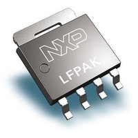
PSMN9R0-25YLC,115 NXP Semiconductors, PSMN9R0-25YLC,115 Datasheet - Page 5

PSMN9R0-25YLC,115
Manufacturer Part Number
PSMN9R0-25YLC,115
Description
MOSFET Power N-chnl25V9.1m logic lvl MOSFET in LFPAK
Manufacturer
NXP Semiconductors
Specifications of PSMN9R0-25YLC,115
Transistor Polarity
N-Channel
Resistance Drain-source Rds (on)
9.1 mOhms
Drain-source Breakdown Voltage
25 V
Gate-source Breakdown Voltage
20 V
Continuous Drain Current
46 A
Power Dissipation
34 W
Maximum Operating Temperature
+ 175 C
Mounting Style
SMD/SMT
Package / Case
LFPAK
Fall Time
5 ns
Gate Charge Qg
12 nC
Minimum Operating Temperature
- 55 C
Rise Time
10 ns
Lead Free Status / Rohs Status
Details
NXP Semiconductors
5. Thermal characteristics
Table 5.
PSMN9R0-25YLC
Product data sheet
Symbol
R
Fig 5.
th(j-mb)
Z
(K/W)
th(j-mb)
10
10
10
-1
-2
1
10
Transient thermal impedance from junction to mounting base as a function of pulse duration
-6
Thermal characteristics
0.05
0.02
δ = 0.5
0.2
0.1
single shot
Parameter
thermal resistance from junction to mounting base
N-channel 25 V 9.1 mΩ logic level MOSFET in LFPAK using NextPower technology
10
-5
All information provided in this document is subject to legal disclaimers.
10
-4
Rev. 2 — 1 November 2011
10
-3
Conditions
see
Figure 5
10
-2
PSMN9R0-25YLC
Min
-
10
P
-1
tp
Typ
4.14
T
© NXP B.V. 2011. All rights reserved.
003aag198
δ =
t
p
Max
4.36
(s)
T
tp
t
1
Unit
K/W
5 of 15


