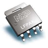
PSMN9R0-25YLC,115 NXP Semiconductors, PSMN9R0-25YLC,115 Datasheet - Page 3

PSMN9R0-25YLC,115
Manufacturer Part Number
PSMN9R0-25YLC,115
Description
MOSFET Power N-chnl25V9.1m logic lvl MOSFET in LFPAK
Manufacturer
NXP Semiconductors
Specifications of PSMN9R0-25YLC,115
Transistor Polarity
N-Channel
Resistance Drain-source Rds (on)
9.1 mOhms
Drain-source Breakdown Voltage
25 V
Gate-source Breakdown Voltage
20 V
Continuous Drain Current
46 A
Power Dissipation
34 W
Maximum Operating Temperature
+ 175 C
Mounting Style
SMD/SMT
Package / Case
LFPAK
Fall Time
5 ns
Gate Charge Qg
12 nC
Minimum Operating Temperature
- 55 C
Rise Time
10 ns
Lead Free Status / Rohs Status
Details
NXP Semiconductors
PSMN9R0-25YLC
Product data sheet
Fig 1.
Fig 3.
(A)
I
D
50
40
30
20
10
0
mounting base temperature
Continuous drain current as a function of
Single pulse avalanche rating; avalanche current as a function of avalanche time
0
50
N-channel 25 V 9.1 mΩ logic level MOSFET in LFPAK using NextPower technology
100
(A)
I
AL
10
10
150
2
1
10
All information provided in this document is subject to legal disclaimers.
-3
003aag195
T
mb
( ° C)
200
Rev. 2 — 1 November 2011
10
-2
10
-1
(2)
(1)
Fig 2.
P
(%)
der
120
80
40
0
1
function of mounting base temperature
Normalized total power dissipation as a
0
003aag196
t
AL
(ms)
10
50
PSMN9R0-25YLC
100
150
© NXP B.V. 2011. All rights reserved.
T
mb
03na19
(°C)
200
3 of 15


