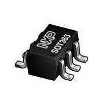
BF1204 NXP Semiconductors, BF1204 Datasheet - Page 2

BF1204
Manufacturer Part Number
BF1204
Description
Two dual-gate MOS Field-Effect Transistors in a plastic SOT363 package
Manufacturer
NXP Semiconductors
Datasheet
1.BF1204.pdf
(13 pages)
Specifications of BF1204
Application
VHF/UHF
Channel Type
N
Channel Mode
Enhancement
Continuous Drain Current
0.03A
Drain Source Voltage (max)
10V
Power Gain (typ)@vds
34@5VdB
Noise Figure (max)
11dB
Package Type
SOT-363
Pin Count
6
Input Capacitance (typ)@vds
1.7@5V@Gate 1/3.3@5V@Gate 2pF
Output Capacitance (typ)@vds
0.85@5VpF
Reverse Capacitance (typ)
0.015@5VpF
Operating Temp Range
-65C to 150C
Mounting
Surface Mount
Number Of Elements
2
Power Dissipation (max)
200mW
Screening Level
Military
Lead Free Status / Rohs Status
Compliant
Available stocks
Company
Part Number
Manufacturer
Quantity
Price
Part Number:
BF1204
Manufacturer:
NXP/恩智浦
Quantity:
20 000
Part Number:
BF1204,115
Manufacturer:
NXP/恩智浦
Quantity:
20 000
NXP Semiconductors
FEATURES
Two low noise gain controlled amplifiers in a single
Superior cross-modulation performance during AGC
High forward transfer admittance
High forward transfer admittance to input capacitance
APPLICATIONS
Gain controlled low noise amplifiers for VHF and UHF
DESCRIPTION
The BF1204 is a combination of two equal dual gate
MOS-FET amplifiers with shared source and gate 2 leads.
The source and substrate are interconnected. Internal bias
circuits enable DC stabilization and a very good
cross-modulation performance during AGC. Integrated
diodes between the gates and source protect against
excessive input voltage surges. The transistor has a
SOT363 micro-miniature plastic package.
QUICK REFERENCE DATA
Note
1. T
2010 Sep 16
Per MOS-FET; unless otherwise specified
V
I
P
y
C
C
NF
X
T
SYMBOL
This product is supplied in anti-static packing to prevent damage caused by electrostatic discharge during transport
and handling.
D
package
ratio.
applications with 3 to 9 V supply voltage, such as digital
and analog television tuners and professional
communications equipment.
j
DS
tot
mod
Dual N-channel dual gate MOS-FET
ig1-s
rss
fs
s
is the temperature at the soldering point of the source lead.
drain-source voltage
drain current (DC)
total power dissipation
forward transfer admittance
input capacitance at gate 1
reverse transfer capacitance
noise figure
cross-modulation
operating junction temperature
PARAMETER
T
I
I
f = 1 MHz
f = 800 MHz
input level for k = 1% at 40 dB AGC 100
D
D
s
= 12 mA; f = 1 MHz
= 12 mA; f = 1 MHz
102 C; note 1
CAUTION
2
CONDITIONS
PINNING - SOT363
handbook, halfpage
Marking code: L3*
Top view
1
6
PIN
1
2
3
4
5
6
Fig.1 Simplified outline and symbol.
5
2
4
3
gate 1 (a)
gate 2
gate 1 (b)
drain (b)
source
drain (a)
25
MIN.
g1 (a)
* = - : made in Hong Kong
* = p : made in Hong Kong
* = t : made in Malaysia
AMP
d (a)
DESCRIPTION
a
30
1.7
15
1.1
105
TYP.
Product specification
g2
s
10
30
200
40
2.2
1.8
150
MAX.
g1 (b)
BF1204
AMP
d (b)
b
MBL252
V
mA
mW
mS
pF
fF
dB
dBV
C
UNIT


