BF904WR NXP Semiconductors, BF904WR Datasheet - Page 2
BF904WR
Manufacturer Part Number
BF904WR
Description
Enhancement type Field-Effect Transistor in a plastic SOT343R package
Manufacturer
NXP Semiconductors
Datasheet
1.BF904WR.pdf
(14 pages)
Specifications of BF904WR
Application
VHF/UHF
Channel Type
N
Channel Mode
Enhancement
Continuous Drain Current
0.03A
Drain Source Voltage (max)
7V
Noise Figure (max)
2.8dB
Frequency (max)
1GHz
Package Type
CMPAK
Pin Count
3 +Tab
Input Capacitance (typ)@vds
2.2@5V@Gate 1/1.5@5V@Gate 2pF
Output Capacitance (typ)@vds
1.3@5VpF
Reverse Capacitance (typ)
0.025@5VpF
Operating Temp Range
-65C to 150C
Mounting
Surface Mount
Number Of Elements
2
Power Dissipation (max)
280mW
Screening Level
Military
Lead Free Status / Rohs Status
Compliant
Available stocks
Company
Part Number
Manufacturer
Quantity
Price
Company:

Part Number:
BF904WR
Manufacturer:
NXP
Quantity:
51 000


NXP Semiconductors
FEATURES
Specially designed for use at 5 V supply voltage
Short channel transistor with high forward transfer
Low noise gain controlled amplifier up to 1 GHz
Superior cross-modulation performance during AGC.
APPLICATIONS
VHF and UHF applications with 3 to 7 V supply voltage
DESCRIPTION
Enhancement type field-effect transistor in a plastic
microminiature SOT343R package. The transistor
consists of an amplifier MOS-FET with source and
substrate interconnected and an internal bias circuit to
ensure good cross-modulation performance during AGC.
QUICK REFERENCE DATA
2010 Sep 15
V
I
P
T
y
C
C
F
The device is supplied in an antistatic package. The
gate-source input must be protected against static
discharge during transport or handling.
D
admittance to input capacitance ratio
such as television tuners and professional
communications equipment.
j
DS
tot
N-channel dual-gate MOS-FET
ig1-s
rs
SYMBOL
fs
drain-source voltage
drain current
total power dissipation
operating junction temperature
forward transfer admittance
input capacitance at gate 1
reverse transfer capacitance
noise figure
CAUTION
PARAMETER
2
PINNING
handbook, halfpage
f = 1 MHz
f = 800 MHz
CONDITIONS
Marking code: MC*
PIN
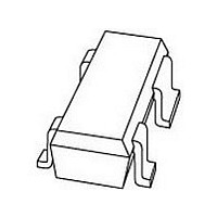
Fig.1 Simplified outline (SOT343R) and symbol.
1
2
3
4
Top view
3
2
SYMBOL
1
s, b
g
g
4
d
2
1
22
MIN.
source
drain
gate 2
gate 1
MAM192
25
2.2
25
2
g 2
g
TYP.
* = - : made in Hong Kong
* = p : made in Hong Kong
* = t : made in Malaysia
1
DESCRIPTION
Product specification
d
7
30
280
150
30
2.6
35
BF904WR
MAX.
s,b
V
mA
mW
C
mS
pF
fF
dB
UNIT
Related parts for BF904WR
Image
Part Number
Description
Manufacturer
Datasheet
Request
R

Part Number:
Description:
MOSFET N-CH 7V 30MA SOT143B
Manufacturer:
NXP Semiconductors
Datasheet:

Part Number:
Description:
Enhancement type Field-Effect Transistor in a plastic SOT143B package
Manufacturer:
NXP Semiconductors
Datasheet:

Part Number:
Description:
RF MOSFET Small Signal TAPE7 MOS-RFSS
Manufacturer:
NXP Semiconductors
Datasheet:
Part Number:
Description:
MOSFET N-CH 7V 30MA SOT143
Manufacturer:
NXP Semiconductors
Datasheet:

Part Number:
Description:
RF MOSFET Power RF MOSFETS
Manufacturer:
Infineon Technologies
Part Number:
Description:
RF MOSFET Power RF MOSFETS
Manufacturer:
Infineon Technologies

Part Number:
Description:
Manufacturer:
Infineon Technologies
Datasheet:

Part Number:
Description:
NXP Semiconductors designed the LPC2420/2460 microcontroller around a 16-bit/32-bitARM7TDMI-S CPU core with real-time debug interfaces that include both JTAG andembedded trace
Manufacturer:
NXP Semiconductors
Datasheet:

Part Number:
Description:
NXP Semiconductors designed the LPC2458 microcontroller around a 16-bit/32-bitARM7TDMI-S CPU core with real-time debug interfaces that include both JTAG andembedded trace
Manufacturer:
NXP Semiconductors
Datasheet:
Part Number:
Description:
NXP Semiconductors designed the LPC2468 microcontroller around a 16-bit/32-bitARM7TDMI-S CPU core with real-time debug interfaces that include both JTAG andembedded trace
Manufacturer:
NXP Semiconductors
Datasheet:
Part Number:
Description:
NXP Semiconductors designed the LPC2470 microcontroller, powered by theARM7TDMI-S core, to be a highly integrated microcontroller for a wide range ofapplications that require advanced communications and high quality graphic displays
Manufacturer:
NXP Semiconductors
Datasheet:
Part Number:
Description:
NXP Semiconductors designed the LPC2478 microcontroller, powered by theARM7TDMI-S core, to be a highly integrated microcontroller for a wide range ofapplications that require advanced communications and high quality graphic displays
Manufacturer:
NXP Semiconductors
Datasheet:
Part Number:
Description:
The Philips Semiconductors XA (eXtended Architecture) family of 16-bit single-chip microcontrollers is powerful enough to easily handle the requirements of high performance embedded applications, yet inexpensive enough to compete in the market for hi
Manufacturer:
NXP Semiconductors
Datasheet:
Part Number:
Description:
The XA-S3 device is a member of Philips Semiconductors? XA(eXtended Architecture) family of high performance 16-bitsingle-chip microcontrollers
Manufacturer:
NXP Semiconductors
Datasheet: