ICS8735AM-21 IDT, Integrated Device Technology Inc, ICS8735AM-21 Datasheet
ICS8735AM-21
Specifications of ICS8735AM-21
Available stocks


Related parts for ICS8735AM-21


ICS8735AM-21 Summary of contents
Page 1
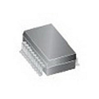
... ICS8735-21 CLK nCLK 2 19 SEL1 SEL0 nFB_IN 5 16 PLL_SEL FB_IN CCA SEL2 7 14 SEL3 nQFB QFB ICS8735-21 20-Lead SOIC M Package Top View ICS8735- 32-Lead VFQFN 5mm x 5mm x 0.925mm package body QFB Package Top View 6 nQFB ICS8735AM-21 REV. A JULY 31, 2008 CCO CCO ...
Page 2
... When LOW, selects reference clock. When HIGH, selects PLL. LVCMOS/LVTTL interface levels. Differential output pair. LVPECL interface levels. Differential feedback output pair. LVPECL interface levels. Negative supply pin. Core supply pins. Analog supply pin. Output supply pin. Test Conditions 2 Minimum Typical Maximum ICS8735AM-21 REV. A JULY 31, 2008 Units pF Ω k Ω k ...
Page 3
... Outputs PLL_SEL = 1 PLL Enable Mode Q/nQ, QFB/nQFB ÷1 ÷1 ÷1 ÷1 ÷2 ÷2 ÷2 ÷4 ÷4 ÷ ICS8735AM-21 REV. A JULY 31, 2008 ...
Page 4
... SEL3 SEL2 SEL1 IDT™ / ICS™ 3.3V LVPECL ZERO DELAY CLOCK GENERATOR Outputs PLL_SEL = 0 PLL Bypass Mode SEL0 Q/nQ, QFB/nQFB 0 ÷4 1 ÷4 0 ÷4 1 ÷8 0 ÷8 1 ÷8 0 ÷16 1 ÷16 0 ÷32 1 ÷64 0 ÷2 1 ÷2 0 ÷4 1 ÷1 0 ÷2 1 ÷1 4 ICS8735AM-21 REV. A JULY 31, 2008 ...
Page 5
... V = 3.465V 3.465V 3.465V 0. 0V 0°C to 70° Typical Maximum 3.3 3.465 3.3 3.465 3.3 3.465 150 0°C to 70° Minimum Typical Maximum 0.3 CC -0.3 0.8 150 5 -5 -150 ICS8735AM-21 REV. A JULY 31, 2008 Units Units V V µA µA µA µA ...
Page 6
... EE A Minimum Typical Maximum V – 1.4 V – 0.9 CCO CCO V – 2.0 V – 1.7 CCO CCO 0.6 1 0°C to 70° Minimum Typical Maximum 31.25 700 700 ICS8735AM-21 REV. A JULY 31, 2008 Units µA µA µA µ Units Units MHz MHz ...
Page 7
... IDT™ / ICS™ 3.3V LVPECL ZERO DELAY CLOCK GENERATOR = 3.3V ± 5 0V, T CCA CCO EE Test Conditions PLL_SEL = 0V, f ≤ 700MHz PLL_SEL = 0V PLL_SEL = 3.3V 20% to 80% @ 50MHz 7 = 0°C to 70°C A Minimum Typical Maximum 700 3.0 4.2 20 -50 50 150 25 ±50 1 300 700 47 53 ICS8735AM-21 REV. A JULY 31, 2008 Units MHz ...
Page 8
... IDT™ / ICS™ 3.3V LVPECL ZERO DELAY CLOCK GENERATOR SCOPE Qx nQx Differential Input Level V nQx nQy Output Skew Clock ➤ ➤ tcycle n+1 Outputs | Output Rise/Fall Time nCLK V Cross Points PP CLK V EE tsk(o) 80% 80% 20 ICS8735AM-21 REV. A JULY 31, 2008 V CMR 20% ...
Page 9
... IDT™ / ICS™ 3.3V LVPECL ZERO DELAY CLOCK GENERATOR nCLK CLK nQ, nQFB x 100% Q, QFB Propagation Delay Outputs: LVPECL Outputs All unused LVPECL outputs can be left floating. We recommend that there is no trace attached. Both sides of the differential output pair should either be left floating or terminated ICS8735AM-21 REV. A JULY 31, 2008 ...
Page 10
... IDT™ / ICS™ 3.3V LVPECL ZERO DELAY CLOCK GENERATOR and V should be CCA CCO CCA / Figure 2. Single-Ended Signal Driving Differential Input 10 3. .01µF 10Ω V CCA .01µF 10µF Figure 1. Power Supply Filtering Single Ended Clock Input CLK V_REF nCLK C1 0. ICS8735AM-21 REV. A JULY 31, 2008 ...
Page 11
... Zo = 50Ω R1 100 Zo = 50Ω LVDS Driven by a 3.3V LVDS Driver 2. 120 120 Zo = 60Ω 60Ω SSTL R1 R2 120 120 Driven by a 2.5V SSTL Driver ICS8735AM-21 REV. A JULY 31, 2008 3.3V CLK nCLK HiPerClockS Input 3.3V CLK nCLK Receiver 3.3V CLK nCLK HiPerClockS ...
Page 12
... FIN FOUT 50Ω RTT Figure 4B. 3.3V LVPECL Output Termination 12 3.3V 125Ω 125Ω 50Ω o FIN Z = 50Ω o 84Ω 84Ω ICS8735AM-21 REV. A JULY 31, 2008 ...
Page 13
... Bypass capacitors located near the power pins (U1-4) VCC=3.3V SEL[3:0] = 0101, Divide VCCA 10 20 C11 nc SEL1 19 0.01u C16 SEL0 18 10u VCC 17 PLL_SEL 16 VCCA 15 SEL3 14 VCC Ohm Ohm (77.75 MHz (U1-17) (U1-13) VCC 0.1uF 0.1uF 0.1uF ICS8735AM-21 REV. A JULY 31, 2008 VCC + - LVPECL_input R5 50 ...
Page 14
... These recommendations are to be used as a guideline only. For further information, please refer to the Application Note on the Surface Mount Assembly of Amkor’s Thermally/Electrically Enhance Leadfame Base Package, Amkor Technology. SOLDER EXPOSED HEAT SLUG LAND PATTERN (GROUND PAD) THERMAL VIA 14 PIN PIN PAD ICS8735AM-21 REV. A JULY 31, 2008 ...
Page 15
... Air Flow JA 0 83.2°C/W 46.2°C/W for 32 Lead VFQFN, Forced Convection JA θ by Velocity JA 0 37.0°C/W 15 must be used. Assuming no air flow JA 200 500 65.7°C/W 57.5°C/W 39.7°C/W 36.8°C/W 1 2.5 32.4°C/W 29.0°C/W ICS8735AM-21 REV. A JULY 31, 2008 ...
Page 16
... IDT™ / ICS™ 3.3V LVPECL ZERO DELAY CLOCK GENERATOR V OUT RL 50Ω CCO = V – 0.9V CCO_MAX = V – 1.7V CCO_MAX ] * (V – [(2V – CCO_MAX OH_MAX ] * (V – [(2V – CCO_MAX OL_MAX 16 – V ))/ CCO_MAX OH_MAX L CCO_MAX – V ))/ CCO_MAX OL_MAX L CCO_MAX ICS8735AM-21 REV. A JULY 31, 2008 – OH_MAX – OL_MAX ...
Page 17
... All Dimensions in Millimeters Symbol Minimum 0.10 A2 2.05 B 0.33 C 0.18 D 12.60 E 7.40 e 1.27 Basic H 10.00 h 0.25 L 0.40 α 0° 17 500 57.5°C/W 36.8°C/W 2.5 29.0°C/W Maximum 2.65 2.55 0.51 0.32 13.00 7.60 10.65 0.75 1.27 7° ICS8735AM-21 REV. A JULY 31, 2008 ...
Page 18
... Reference Document: JEDEC Publication 95, MO-220 IDT™ / ICS™ 3.3V LVPECL ZERO DELAY CLOCK GENERATOR -1 ef Anvil Singula tion (Ref.) N & N Odd Maximum 1.00 0.05 0.30 3.3 0.50 18 (Ref.) N & N Even N e (Ty p & are Even 2 (N -1)x e (Re f mal ICS8735AM-21 REV. A JULY 31, 2008 ...
Page 19
... Tape & Reel “Lead-Free” 32 Lead VFQFN “Lead-Free” 32 Lead VFQFN 2500 Tape & Reel 19 Temperature Tube 0°C to 70°C 0°C to 70°C Tube 0°C to 70°C 0°C to 70°C Tray 0°C to 70°C 0°C to 70°C ICS8735AM-21 REV. A JULY 31, 2008 ...
Page 20
ICS8735-21 700MHZ, DIFFERENTIAL-TO-3.3V LVPECL ZERO DELAY CLOCK GENERATOR Contact Information: www.IDT.com Sales 800-345-7015 (inside USA) +408-284-8200 (outside USA) Fax: 408-284-2775 www.IDT.com/go/contactIDT © 2008 Integrated Device Technology, Inc. All rights reserved. Product specifications subject to change without notice. IDT and the ...