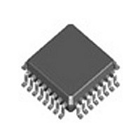
ICS83940DYI IDT, Integrated Device Technology Inc, ICS83940DYI Datasheet - Page 6

ICS83940DYI
Manufacturer Part Number
ICS83940DYI
Description
Manufacturer
IDT, Integrated Device Technology Inc
Type
Clock Driverr
Datasheet
1.ICS83940DYI.pdf
(19 pages)
Specifications of ICS83940DYI
Number Of Clock Inputs
2
Output Frequency
250MHz
Output Logic Level
LVCMOS/LVTTL
Operating Supply Voltage (min)
2.375V
Operating Supply Voltage (typ)
2.5/3.3V
Operating Supply Voltage (max)
3.465V
Package Type
LQFP
Operating Temp Range
-40C to 85C
Operating Temperature Classification
Industrial
Mounting
Surface Mount
Pin Count
32
Lead Free Status / Rohs Status
Not Compliant
Available stocks
Company
Part Number
Manufacturer
Quantity
Price
Company:
Part Number:
ICS83940DYI-01LF
Manufacturer:
IDT, Integrated Device Technology Inc
Quantity:
10 000
Company:
Part Number:
ICS83940DYI-01LFT
Manufacturer:
IDT, Integrated Device Technology Inc
Quantity:
10 000
Company:
Part Number:
ICS83940DYILF
Manufacturer:
IDT
Quantity:
4 218
Company:
Part Number:
ICS83940DYILF
Manufacturer:
IDT, Integrated Device Technology Inc
Quantity:
10 000
Company:
Part Number:
ICS83940DYILFT
Manufacturer:
IDT, Integrated Device Technology Inc
Quantity:
10 000
ICS83940DI Data Sheet
AC Electrical Characteristics
Table 5A. AC Characteristics, V
NOTE: Electrical parameters are guaranteed over the specified ambient operating temperature range, which is established when the device is
mounted in a test socket with maintained transverse airflow greater than 500 lfpm. The device will meet specifications after thermal equilibrium
has been reached under these conditions.
NOTE: All parameters measured at 200MHz unless noted otherwise.
NOTE 1: Measured from the differential input crossing point to the output V
NOTE 2: Measured from V
NOTE 3: Defined as skew between outputs at the same supply voltage and with equal load conditions. Measured at V
NOTE 4: Defined as skew between outputs on different devices operating at the same supply voltage, same temperature and with equal load
conditions. Using the same type of inputs on each device, the outputs are measured at V
NOTE 5: This parameter is defined in accordance with JEDEC Standard 65.
NOTE 6: Defined as skew between outputs on different devices, across temperature and voltage ranges, and with equal load conditions. Using
the same type of inputs on each device, the outputs are measured at V
ICS83940DYI REVISION C SEPTEMBER 7, 2010
Symbol
f
t
tsk(o)
tsk(pp)
t
odc
MAX
PLH
R
/ t
F
Parameter
Output Frequency
Propagation
Delay
Propagation
Delay
Output Skew;
NOTE 3, 5
Part-to-Part Skew;
NOTE 6
Part-to-Part Skew;
NOTE 6
Part-to-Part Skew;
NOTE 4, 5
Output Rise/Fall Time
Output Duty Cycle
DD
/2 to V
PCLK, nPCLK; NOTE 1, 5
LVCMOS_CLK; NOTE 2, 5
PCLK, nPCLK; NOTE 1, 5
LVCMOS_CLK; NOTE 2, 5
PCLK, nPCLK
LVCMOS_CLK
PCLK, nPCLK
LVCMOS_CLK
PCLK, nPCLK
LVCMOS_CLK
PCLK, nPCLK
LVCMOS_CLK
DDO
DD
/2.
= V
DDO
= 3.3V ± 5%, T
Measured on the Rising Edge
Measured on the Rising Edge
A
134MHz ≤ ƒ ≤ 250MHz
= -40°C to 85°C
Test Conditions
6
DDO
ƒ > 150MHz
ƒ > 150MHz
ƒ > 150MHz
ƒ > 150MHz
0.5V to 2.4V
ƒ < 134MHz
ƒ ≤ 150MHz
ƒ ≤ 150MHz
ƒ ≤ 150MHz
ƒ ≤ 150MHz
@ V
@ V
DDO
/2.
DDO
DDO
/2.
LOW SKEW, 1-TO-18 LVPECL-TO-LVCMOS/LVTTL FANOUT BUFFER
/2
/2
DDO
/2.
Minimum
0.3
1.6
1.8
1.6
1.8
45
40
©2010 Integrated Device Technology, Inc.
Typical
50
50
DDO
Maximum
/2.
250
150
150
850
750
3.0
3.0
3.3
3.2
1.4
1.2
1.7
1.4
1.1
55
60
Units
MHz
ns
ns
ns
ns
ps
ps
ns
ns
ns
ns
ps
ps
ns
%
%


