KA3504 Fairchild Semiconductor, KA3504 Datasheet

KA3504

Manufacturer Part Number
KA3504
Description
Manufacturer
Fairchild Semiconductor
Datasheet

Specifications of KA3504

Number Of Elements
1
Battery Backup Switching
No
Watchdog Timer
No
Chip Enable Signals
No
Manual Reset
No
Package Type
PDIP
Operating Supply Voltage (min)
15V
Operating Supply Voltage (max)
30V
Power Dissipation
1W
Operating Temp Range
-25C to 85C
Operating Temperature Classification
Commercial
Power Fail Detection
Yes
Mounting
Through Hole
Pin Count
16
Supply Current
10mA
Lead Free Status / Rohs Status
Compliant

Available stocks

Company
Part Number
Manufacturer
Quantity
Price
Part Number:
KA3504
Manufacturer:
FAIRCHILD/仙童
Quantity:
20 000
Features
• PC Power Supply Output Monitor Circuitry
• Few External Components
• Over Voltage Protection for 3.3V/5V/12V Output
• Over Current Protection for 3.3V/5V/12V Output With
• Fault Protection Output With Open Collector Output
• Power Supply on/off Delay Time Control (PSON)
• Power Good Signal Generator With Hysteresis
• Open Collector PG Output
• 300ms Power Good Delay
• Current Sense Setting Function With RI
• Latch Function Controlled by PSON and Protection Input
• 16-Pin Dual In-line Package
FPO (Fault Protection Output)
Fault Protection Output indicates the fault condition as
protection signal. When fault state occurs, the main power is
to be turned-off and the PGO signal goes LOW.
NORMAL = "LOW", FAULT = "HIGH"
PGO (Power Good Output)
Power Good Signal Generator is to monitor the voltage level
of power supply for safe operation of a microprocessor
having some delay time at turn-on. The delay time is
prorammed by a timing capacitor connected to TPG pin of
KA3504. The power good output should be low state before
the output voltage is out of regulation at turn-off.
NORMAL = "HIGH", FAULT = "LOW"
©2002 Fairchild Semiconductor Corporation
KA3504
PC SMPS Supervisory IC
Delay Time
Description
The KA3504 is complete output supervisory circuitry
intended for use in the secondary side of the switched mode
power supply. It provides all the functions necessary to
monitor and control the output of the power supply system.
Power good signal generator, Remote on and off control,
some precision protection features against over-voltage and
over-current are implemented. It directly senses all the
output rails for OVP without any external dividers. As for
output control, power good output (PGO) and Fault
Protection output (FPO) are also included. Utilizing a
minimum number of external components, the KA3504
offers a simple and cost effective solution, greatly reducing
PCB board space for power supply system.
OCP (Over Current Protection)
It has precision OCP functions for +3.3V, +5V, +12V
outputs. The block is made up of three comparators with
current source setting function. Two inputs of each OCP
comparator are connected to both sides of output inductor
that is located in the secondary output of SMPS.
OVP (Over Voltage Protection)
It has OVP functions for +3.3V, +5V, +12V outputs.
The circuit is made up of a comparator with three detecting
inputs.
Remote ON/OFF
Remote on/off section is used to control SMPS externally.
If a high signal is supplied to the remote on/off input, FPO
signal becomes a high state and all secondary outputs are
grounded. The remote on/off signal is transferred with some
on-delay and off-delay time of 8ms, 24ms respectively with
0.1 F external capacitor.
16-DIP
1
www.fairchildsemi.com
Rev. 1.0.1

Related parts for KA3504

KA3504 Summary of contents

Page 1

... The delay time is prorammed by a timing capacitor connected to TPG pin of KA3504. The power good output should be low state before the output voltage is out of regulation at turn-off. NORMAL = "HIGH", FAULT = "LOW" ...

Page 2

... KA3504 Internal Block Diagram 3 VS12 OVP VS5 2 Detector VS33 1 COMP1 1 4 IS12 Iref*5 (100uA) COMP2 IS5 1 5 Iref*5 (100uA) IS33 1 6 Iref*5 COMP3 (100uA) Absolute Maximum Ratings Parameter Supply Voltage Input Voltage FPO Voltage FPO Maximum Current Operating Temperature Storage Temperature Range ...

Page 3

... Pin Assignments : KA3504 VS33 VS5 VS12 PGI Vcc FPO PSON T PSON KA3504 IS33 IS5 IS12 T PROT GND PGO 3 ...

Page 4

... KA3504 Pin Definitions Pin No. Name Over Voltage Protection Input for the 3.3V. It Directly Senses the 3.3V Rail 1 VS33 Without any External Divider. Over Voltage Protection Input for the 5V. It Directly Senses the 5V Rail Without 2 VS5 any External Divider. Over Voltage Protection Input for the 12V. It Directly Senses the 12V Rail ...

Page 5

... C = 0.1 F OFF(PSON 10mA SAT(FPO) FPO 20V LKG(FPO) FPO Symbol Test Conditions V PG: "H" "L" IN(PG1) HY1 COMP7 HY2 COMP4 CHG(PG 2.2 F D(PG 10mA SAT(PG KA3504 Min. Typ. Max. Unit 3.9 4.1 4.3 V 5.7 6.1 6.5 V 13.6 14.3 15 -15 -21 - msec 1 1.4 1 5.25 ...

Page 6

... KA3504 Timing / Housekeeping / Control Remote on/off Output Voltage (3.3V, 5V, 12V) PGO FPO Stand-by Mode Vcc Power on/off 6 Toff Delay PG Delay Operating Mode PGI Detection Point Main Power Switch ON Ton Delay PG Delay OFF ...

Page 7

... Test Circuit KA3504 7 ...

Page 8

... KA3504 Typical Characteristics 0.006 0.005 Icc=4.881mA Vcc=20V 0.004 0.003 0.002 0.001 0.000 Vcc[V] Figure 5.4 5.6 5.8 6.0 5V Output Voltage[V] Figure 3. Over Voltage Protection for +5V 0.000010 0.000005 0.000000 -0.000005 -0.000010 -0.000015 -0.000020 PSON Voltage[V] Figure 5. PS On/Off Delay Current 8 Icc 20 15 ...

Page 9

... PGI Voltage[V] PGI Voltage[V] Figure 7. Hysteresis Voltage 1 (Continued) HY1 HY1 1.3 1.3 1.4 1.4 1.5 1.5 0.0 0.0 HY2 HY2 0.5 0.5 1.0 1.0 1.5 1.5 2.0 2.0 2.5 2.5 TPG Voltage[V] TPG Voltage[V] Figure 8. Hysteresis Voltage 2 KA3504 9 ...

Page 10

... KA3504 Application Circuit C109 C110 TX2 C112 N C115 1 D11 R32 10 2 TX4 8 C119 D13 R38 D14 C124 D15 Vcc R27 C103 2 TX1 SW2 C106 R28 C111 D10 R30 B+ TX3 2 1 Lp1 Ls C116 R33 D12 2 Vcc1 C118 M1 PWM IC R39 2 1 R41 C122 ...

Page 11

... Mechanical Dimensions Package 6.40 0.20 0.252 0.008 #1 #16 #8 7.62 0.300 16-DIP #9 3.25 0.20 0.128 0.008 5.08 MAX 0.200 Dimensions in millimeters 0.38 MIN 0.014 3.30 0.30 0.130 0.012 KA3504 11 ...

Page 12

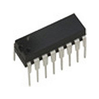
... KA3504 Ordering Information Product Number Package KA3504 16-DIP DISCLAIMER FAIRCHILD SEMICONDUCTOR RESERVES THE RIGHT TO MAKE CHANGES WITHOUT FURTHER NOTICE TO ANY PRODUCTS HEREIN TO IMPROVE RELIABILITY, FUNCTION OR DESIGN. FAIRCHILD DOES NOT ASSUME ANY LIABILITY ARISING OUT OF THE APPLICATION OR USE OF ANY PRODUCT OR CIRCUIT DESCRIBED HEREIN; NEITHER DOES IT CONVEY ANY LICENSE UNDER ITS PATENT RIGHTS, NOR THE RIGHTS OF OTHERS ...

Related keywords