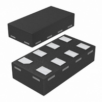
74LVCV2G66GD,125 NXP Semiconductors, 74LVCV2G66GD,125 Datasheet - Page 5

74LVCV2G66GD,125
Manufacturer Part Number
74LVCV2G66GD,125
Description
IC SWITCH DUAL SPST 8XSON
Manufacturer
NXP Semiconductors
Type
Analog Switchr
Datasheet
1.74LVCV2G66GD125.pdf
(23 pages)
Specifications of 74LVCV2G66GD,125
Package / Case
8-XSON
Function
Switch
Circuit
2 x SPST - NO
On-state Resistance
7.3 Ohm
Voltage Supply Source
Single Supply
Voltage - Supply, Single/dual (±)
2.3 V ~ 5.5 V
Current - Supply
0.1µA
Operating Temperature
-40°C ~ 125°C
Mounting Type
Surface Mount
On Resistance (max)
13 Ohms
On Time (max)
4.7 ns
Off Time (max)
7.9 ns
Supply Voltage (max)
5.5 V
Supply Voltage (min)
2.3 V
Maximum Power Dissipation
250 mW
Maximum Operating Temperature
+ 125 C
Mounting Style
SMD/SMT
Minimum Operating Temperature
- 40 C
Propagation Delay Time
0.2 ns, 0.3 ns, 0.4 ns
Switch Current (typ)
0.0001 mA
Package
8XSON8U
Maximum On Resistance
30@2.7V Ohm
Maximum Propagation Delay Bus To Bus
0.2(Typ)@5.5V|0.3(Typ)@3.6V|0.4(Typ)@2.7V ns
Maximum Low Level Output Current
50 mA
Maximum Turn-off Time
7.9(Typ)@2.7V ns
Maximum Turn-on Time
4.7(Typ)@2.7V ns
Switch Architecture
SPST
Power Supply Type
Single
Lead Free Status / RoHS Status
Lead free / RoHS Compliant
Lead Free Status / RoHS Status
Lead free / RoHS Compliant, Lead free / RoHS Compliant
Other names
74LVCV2G66GD-G
74LVCV2G66GD-G
935286865125
74LVCV2G66GD-G
935286865125
Available stocks
Company
Part Number
Manufacturer
Quantity
Price
Company:
Part Number:
74LVCV2G66GD,125
Manufacturer:
Vishay
Quantity:
3 298
NXP Semiconductors
10. Static characteristics
Table 7.
At recommended operating conditions; voltages are referenced to GND (ground = 0 V).
[1]
[2]
[3]
74LVCV2G66
Product data sheet
Symbol Parameter
V
V
I
I
I
I
ΔI
C
C
C
I
S(OFF)
S(ON)
CC
IH
IL
I
S(OFF)
S(ON)
CC
All typical values are measured at T
These typical values are measured at V
For overvoltage signals (V
HIGH-level
input voltage
LOW-level
input voltage
input leakage
current
OFF-state
leakage
current
ON-state
leakage
current
supply
current
additional
supply
current
input
capacitance
OFF-state
capacitance
ON-state
capacitance
Static characteristics
Conditions
V
V
V
V
V
V
pin nE; V
V
V
V
V
V
V
pin nE; V
V
V
CC
CC
CC
CC
CC
CC
CC
CC
CC
I
SW
CC
SW
CC
SW
= 5.5 V or GND;
= 2.3 V to 2.7 V
= 3.0 V to 3.6 V
= 4.5 V to 5.5 V
= 2.3 V to 2.7 V
= 3.0 V to 3.6 V
= 4.5 V to 5.5 V
= 0 V to 5.5 V
= 2.3 V to 5.5 V; see
= 2.3 V to 5.5 V; see
= 2.3 V to 5.5 V
= 3.0 V to 5.5 V
= GND or V
= GND or V
> V
CC
I
I
= 5.5 V or GND;
= V
) the condition V
amb
CC
CC
= 25 °C.
CC
CC
− 0.6 V;
All information provided in this document is subject to legal disclaimers.
= 3.3 V.
;
;
Y
Figure 6
Figure 7
Rev. 3 — 16 June 2010
< V
Z
must be observed.
[2][3]
[2][3]
[2]
[2]
[2]
0.55V
0.6V
Min
2.0
-
-
-
-
-
-
-
-
-
-
-
−40 °C to +85 °C
CC
CC
Typ
Overvoltage tolerant bilateral switch
±0.1
±0.1
±0.1
0.1
0.1
2.5
8.0
16
-
-
-
-
-
-
[1]
0.15V
0.1V
Max
±10
±10
0.5
±5
10
5
-
-
-
-
-
-
74LVCV2G66
CC
CC
−40 °C to +125 °C Unit
0.55V
0.6V
Min
2.0
-
-
-
-
-
-
-
-
-
-
-
CC
© NXP B.V. 2010. All rights reserved.
CC
0.15V
0.1V
Max
±10
±10
0.5
50
±5
40
-
-
-
-
-
-
CC
CC
5 of 23
V
V
V
V
V
V
μA
μA
μA
μA
μA
pF
pF
pF


