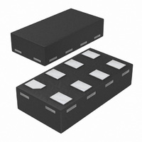
74LVCV2G66GD,125 NXP Semiconductors, 74LVCV2G66GD,125 Datasheet - Page 18

74LVCV2G66GD,125
Manufacturer Part Number
74LVCV2G66GD,125
Description
IC SWITCH DUAL SPST 8XSON
Manufacturer
NXP Semiconductors
Type
Analog Switchr
Datasheet
1.74LVCV2G66GD125.pdf
(23 pages)
Specifications of 74LVCV2G66GD,125
Package / Case
8-XSON
Function
Switch
Circuit
2 x SPST - NO
On-state Resistance
7.3 Ohm
Voltage Supply Source
Single Supply
Voltage - Supply, Single/dual (±)
2.3 V ~ 5.5 V
Current - Supply
0.1µA
Operating Temperature
-40°C ~ 125°C
Mounting Type
Surface Mount
On Resistance (max)
13 Ohms
On Time (max)
4.7 ns
Off Time (max)
7.9 ns
Supply Voltage (max)
5.5 V
Supply Voltage (min)
2.3 V
Maximum Power Dissipation
250 mW
Maximum Operating Temperature
+ 125 C
Mounting Style
SMD/SMT
Minimum Operating Temperature
- 40 C
Propagation Delay Time
0.2 ns, 0.3 ns, 0.4 ns
Switch Current (typ)
0.0001 mA
Package
8XSON8U
Maximum On Resistance
30@2.7V Ohm
Maximum Propagation Delay Bus To Bus
0.2(Typ)@5.5V|0.3(Typ)@3.6V|0.4(Typ)@2.7V ns
Maximum Low Level Output Current
50 mA
Maximum Turn-off Time
7.9(Typ)@2.7V ns
Maximum Turn-on Time
4.7(Typ)@2.7V ns
Switch Architecture
SPST
Power Supply Type
Single
Lead Free Status / RoHS Status
Lead free / RoHS Compliant
Lead Free Status / RoHS Status
Lead free / RoHS Compliant, Lead free / RoHS Compliant
Other names
74LVCV2G66GD-G
74LVCV2G66GD-G
935286865125
74LVCV2G66GD-G
935286865125
Available stocks
Company
Part Number
Manufacturer
Quantity
Price
Company:
Part Number:
74LVCV2G66GD,125
Manufacturer:
Vishay
Quantity:
3 298
NXP Semiconductors
Fig 22. Package outline SOT765-1 (VSSOP8)
74LVCV2G66
Product data sheet
VSSOP8: plastic very thin shrink small outline package; 8 leads; body width 2.3 mm
DIMENSIONS (mm are the original dimensions)
Notes
1. Plastic or metal protrusions of 0.15 mm maximum per side are not included.
2. Plastic or metal protrusions of 0.25 mm maximum per side are not included.
UNIT
mm
OUTLINE
VERSION
SOT765-1
max.
A
1
0.15
0.00
A 1
8
1
Z
0.85
0.60
A 2
y
IEC
e
0.12
A 3
pin 1 index
D
0
0.27
0.17
b p
b p
All information provided in this document is subject to legal disclaimers.
MO-187
0.23
0.08
5
4
JEDEC
c
w
REFERENCES
D
2.1
1.9
M
(1)
Rev. 3 — 16 June 2010
E
2.4
2.2
(2)
c
JEITA
scale
2.5
0.5
e
A
H E
3.2
3.0
A 2
detail X
A 1
0.4
L
H E
E
0.40
0.15
L p
Overvoltage tolerant bilateral switch
0.21
0.19
Q
5 mm
L
L p
PROJECTION
EUROPEAN
Q
0.2
v
74LVCV2G66
A
(A 3 )
0.13
w
X
θ
v
M
0.1
y
© NXP B.V. 2010. All rights reserved.
A
ISSUE DATE
02-06-07
Z
0.4
0.1
(1)
SOT765-1
8°
0°
θ
18 of 23


