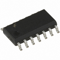
MM74HC4066M Fairchild Semiconductor, MM74HC4066M Datasheet

MM74HC4066M
Specifications of MM74HC4066M
Available stocks
Related parts for MM74HC4066M
MM74HC4066M Summary of contents
Page 1
... Package Order Number Number MM74HC4066M M14A MM74HC4066SJ M14D MM74HC4066MTC MTC14 MM74HC4066N N14A Device also available in Tape and Reel. Specify by appending suffix letter “X” to the ordering number. All packages are lead free per JEDEC: J-STD-020B standard. ©1984 Fairchild Semiconductor Corporation MM74HC4066 Rev. 1.5.0 ...
Page 2
... Connection Diagram Top View Schematic Diagram ©1984 Fairchild Semiconductor Corporation MM74HC4066 Rev. 1.5.0 Truth Table Input Switch CTL I/O–O/I L “OFF” H “ON” 2 www.fairchildsemi.com ...
Page 3
... Supply Voltage Input or Output Voltage IN OUT T Operating Temperature Range Input Rise or Fall Times 2. 4. 6.0V CC ©1984 Fairchild Semiconductor Corporation MM74HC4066 Rev. 1.5.0 (1) Parameter Parameter 3 Rating –0.5 to +15V –1 +1. –0 +0. ±20mA ±25mA ±50mA –65°C to +150°C 600mW 500mW 260°C Min. ...
Page 4
... The worst case leakage current occurs for CMOS at the higher voltage and so the IH 5.5V values should be used supply voltages (V –GND) approaching 2V the analog switch on resistance becomes extremely non-linear. CC Therefore it is recommended that these devices be used to transmit digital only when using these supply voltages. ©1984 Fairchild Semiconductor Corporation MM74HC4066 Rev. 1.5.0 ( (V) Conditions Typ ...
Page 5
... Input Capacitance C Maximum Switch IN Input Capacitance C Maximum Feedthrough IN Capacitance C Power Dissipation PD Capacitance Notes: 5. Adjust 0dBm for F 1kHz (Null centered Adjust input for 0dBm. ©1984 Fairchild Semiconductor Corporation MM74HC4066 Rev. 1.5.0 = 50pF (unless otherwise specified (V) Conditions Typ. CC 2.0V 25 4.5V 5 9.0V 4 12. ...
Page 6
... AC Test Circuits and Switching Time Waveforms Figure 1. “ON” Resistance Figure 4. t PHL Figure 5. t ©1984 Fairchild Semiconductor Corporation MM74HC4066 Rev. 1.5.0 Figure 2. “ON” Channel Leakage Current Figure 3. “OFF” Channel Leakage Current , t Propagation Delay Time Signal Input to Signal Output ...
Page 7
... Figure 6. t Figure 8. Crosstalk: Control Input to Signal Output ©1984 Fairchild Semiconductor Corporation MM74HC4066 Rev. 1.5 Propagation Delay Time Control to Signal Output PZH PHZ Figure 7. Frequency Response 7 www.fairchildsemi.com ...
Page 8
... Figure 10. Switch OFF Signal Feedthrough Isolation ©1984 Fairchild Semiconductor Corporation MM74HC4066 Rev. 1.5.0 Figure 9. Crosstalk Between Any Two Switches Figure 11. Sinewave Distortion 8 www.fairchildsemi.com ...
Page 9
... CC the analog switch input pins, the voltage drop across the switch must not exceed 0.6V (calculated from the ON resistance). ©1984 Fairchild Semiconductor Corporation MM74HC4066 Rev. 1.5.0 Typical Crosstalk Between Any Two Switches Typical Frequency Response 9 www ...
Page 10
... Package drawings are provided as a service to customers considering Fairchild components. Drawings may change in any manner without notice. Please note the revision and/or date on the drawing and contact a Fairchild Semiconductor representative to verify or obtain the most recent revision. Package specifications do not expand the terms of Fairchild’s worldwide terms and conditions, specifi ...
Page 11
... Package drawings are provided as a service to customers considering Fairchild components. Drawings may change in any manner without notice. Please note the revision and/or date on the drawing and contact a Fairchild Semiconductor representative to verify or obtain the most recent revision. Package specifications do not expand the terms of Fairchild’s worldwide terms and conditions, specifi ...
Page 12
... Package drawings are provided as a service to customers considering Fairchild components. Drawings may change in any manner without notice. Please note the revision and/or date on the drawing and contact a Fairchild Semiconductor representative to verify or obtain the most recent revision. Package specifications do not expand the terms of Fairchild’s worldwide terms and conditions, specifi ...
Page 13
... Package drawings are provided as a service to customers considering Fairchild components. Drawings may change in any manner without notice. Please note the revision and/or date on the drawing and contact a Fairchild Semiconductor representative to verify or obtain the most recent revision. Package specifications do not expand the terms of Fairchild’s worldwide terms and conditions, specifi ...
Page 14
... TRADEMARKS The following includes registered and unregistered trademarks and service marks, owned by Fairchild Semiconductor and/or its global subsidiaries, and is not intended exhaustive list of all such trademarks. ® ACEx Build it Now™ CorePLUS™ CROSSVOLT™ CTL™ Current Transfer Logic™ ...


