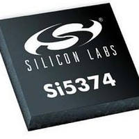
SI5374B-A-GL Silicon Laboratories Inc, SI5374B-A-GL Datasheet - Page 54

SI5374B-A-GL
Manufacturer Part Number
SI5374B-A-GL
Description
Clock Synthesizer / Jitter Cleaner QUAD DSPLL JITT ATT CLK LO LP BW 8IN/OUT
Manufacturer
Silicon Laboratories Inc
Datasheet
1.SI5374B-A-GL.pdf
(64 pages)
Specifications of SI5374B-A-GL
Package / Case
PBGA-80
Input Level
LVCMOS
Max Input Freq
525 Hz
Max Output Freq
808 MHz
Maximum Operating Temperature
+ 85 C
Minimum Operating Temperature
- 40 C
Number Of Outputs
8
Output Level
LVCMOS
Supply Current
1100 mA
Supply Voltage (max)
2.8 V
Supply Voltage (min)
- 0.5 V
Lead Free Status / Rohs Status
Compliant
Available stocks
Company
Part Number
Manufacturer
Quantity
Price
Company:
Part Number:
SI5374B-A-GL
Manufacturer:
SILICON
Quantity:
1 001
Company:
Part Number:
SI5374B-A-GL
Manufacturer:
Silicon Laboratories Inc
Quantity:
10 000
Si5374
Note: Internal register names are indicated by italics, e.g., IRQ_PIN . See Si5374 Register Map.
54
C1, C4, B5
A7, D5, D7
E7, F5, G9
E3, F3, J3
Pin #
D4
D6
B4
D8
H6
E5
E6
F6
F4
F2
Pin Name
RSTL_C
RSTL_D
RSTL_A
RSTL_B
VDD_A
OSC_N
VDD_B
VDD_C
VDD_D
OSC_P
IRQ_C
IRQ_D
IRQ_A
IRQ_B
V
I/O
O
DD
I
I
Table 9. Si5374 Pin Descriptions
LVCMOS External Reset.
LVCMOS DSPLLq Interrupt Indicator.
Analog
Signal
Supply
Level
Preliminary Rev. 0.4
Active low input that performs external hardware reset of all four
DSPLLs. Resets all internal logic to a known state and forces the
device registers to their default value. Clock outputs are tri-stated
during reset. The part must be programmed after a reset or
power-on to get a clock output. This pin has a weak pull-up.
This pin functions as a device interrupt output. The interrupt out-
put, IRQ_PINn must be set to 1. The pin functions as a maskable
interrupt output with active polarity controlled by the IRQ_POLn
register bit.
0 = CKINn present
1 = LOS (FOS) on CKINn
The active polarity is controlled by CK_BAD_POL. If no function
is selected, the pin tri-states.
The device operates from a 1.8 or 2.5 V supply. A 0.1 µF bypass
capacitive is required for every VDD_9 pin. Bypass capacitors
should be associated with the following VDD_q pins:
0.1 µF per VDD pin.
Four 1.0 µF should also be placed as close to each VDD domain
as is practical. See recommended layout.
An external low jitter reference clock should be connected to
these pins. See the any-frequency precision clocks family refer-
ence manual for oscillator selection details.
Supply.
External OSC.
Description


