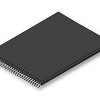
S29GL256S10TFI010 Spansion Inc., S29GL256S10TFI010 Datasheet - Page 65

S29GL256S10TFI010
Manufacturer Part Number
S29GL256S10TFI010
Description
Flash 256 MBIT 3V 100NS PAGE MODE FLASH
Manufacturer
Spansion Inc.
Datasheet
1.S29GL256S10TFI010.pdf
(97 pages)
Specifications of S29GL256S10TFI010
Data Bus Width
16 bit
Memory Type
Flash
Memory Size
256 Mbit
Architecture
Uniform
Timing Type
Asynchronous
Interface Type
CFI
Access Time
100 ns
Supply Voltage (max)
3.6 V
Supply Voltage (min)
2.7 V
Maximum Operating Current
100 mA
Operating Temperature
- 40 C to + 85 C
Mounting Style
SMD/SMT
Package / Case
TSOP-56
Lead Free Status / Rohs Status
Compliant
Available stocks
Company
Part Number
Manufacturer
Quantity
Price
Company:
Part Number:
S29GL256S10TFI010
Manufacturer:
Spansion
Quantity:
25
Hardware Interface
7. Signal Descriptions
7.1
7.2
7.3
7.4
February 11, 2011 S29GL_128S_01GS_00_01
Address and Data Configuration
Input/Output Summary
Versatile I/O Feature
Ready/Busy# (RY/BY#)
Address and data are connected in parallel (ADP) via separate signal inputs and I/Os.
The maximum output voltage level driven by, and input levels acceptable to, the device are determined by the
V
same bus having interface signal levels different from the device core voltage.
RY/BY# is a dedicated, open drain output pin that indicates whether an Embedded Algorithm, Power-On
Reset (POR), or Hardware Reset is in progress or complete. The RY/BY# status is valid after the rising edge
of the final WE# pulse in a command sequence, when V
RESET#
CE#
OE#
WE#
A
DQ15-DQ0
WP#
RY/BY#
V
V
V
NC
RFU
DNU
IO
MAX
CC
IO
SS
D a t a
power supply. This supply allows the device to drive and receive signals to and from other devices on the
-A0
Symbol
S h e e t
Output - open drain
Input
Input
Input
Input
Input
Input/Output
Input
Power Supply
Power Supply
Power Supply
No Connect
No Connect
Reserved
Type
( A d v a n c e
GL-S MirrorBit
Hardware Reset. At V
for reading array data.
Chip Enable. At V
Output Enable. At V
high impedance (High-Z).
Write Enable. At V
transfer is from device to host.
Address inputs.
A25-A0 for S29GL01GS
A24-A0 for S29GL512S
A23-A0 for S29GL256S
A22-A0 for S29GL128S
Data inputs and outputs
Write Protect. At V
64 kword (128 kB) sector of the device. At V
internal pull up; When unconnected WP# is at V
Ready/Busy. Indicates whether an Embedded Algorithm is in progress or complete. At V
the device is actively engaged in an Embedded Algorithm such as erasing or programming.
At High-Z, the device is ready for read or a new command write - requires external pull-up
resistor to detect the High-Z state. Multiple devices may have their RY/BY# outputs tied
together to detect when all devices are ready.
Core power supply
Versatile IO power supply.
Power supplies ground
Not Connected internally. The pin/ball location may be used in Printed Circuit Board (PCB)
as part of a routing channel.
Reserved for Future Use. Not currently connected internally but the pin/ball location should
be left unconnected and unused by PCB routing channel for future compatibility. The pin/ball
may be used by a signal in the future.
Do Not Use. Reserved for use by Spansion. The pin/ball is connected internally. The input
has an internal pull down resistance to V
the PCB.
Table 7.1 I/O Summary
I n f o r m a t i o n )
®
Family
IL
IL
IL
, selects the device for data transfer with the host memory controller.
IL
, indicates data transfer from host to device. At V
, disables program and erase functions in the lowest or highest address
, causes outputs to be actively driven. At V
IL
, causes the device to reset control logic to its standby state, ready
CC
is above V
Description
SS
CC
. The pin/ball can be left open or tied to V
IH
, the sector is not protected. WP# has an
minimum during POR, or after the
IH
.
IH
, causes outputs to be
IH
, indicates data
SS
on
IL
65
,


