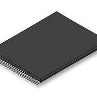
S29GL256S10TFI010 Spansion Inc., S29GL256S10TFI010 Datasheet - Page 30

S29GL256S10TFI010
Manufacturer Part Number
S29GL256S10TFI010
Description
Flash 256 MBIT 3V 100NS PAGE MODE FLASH
Manufacturer
Spansion Inc.
Datasheet
1.S29GL256S10TFI010.pdf
(97 pages)
Specifications of S29GL256S10TFI010
Data Bus Width
16 bit
Memory Type
Flash
Memory Size
256 Mbit
Architecture
Uniform
Timing Type
Asynchronous
Interface Type
CFI
Access Time
100 ns
Supply Voltage (max)
3.6 V
Supply Voltage (min)
2.7 V
Maximum Operating Current
100 mA
Operating Temperature
- 40 C to + 85 C
Mounting Style
SMD/SMT
Package / Case
TSOP-56
Lead Free Status / Rohs Status
Compliant
Available stocks
Company
Part Number
Manufacturer
Quantity
Price
Company:
Part Number:
S29GL256S10TFI010
Manufacturer:
Spansion
Quantity:
25
30
Notes:
1. DQ7 should be rechecked even if DQ5 = 1 because DQ7 may change simultaneously with DQ5.
2. If this flowchart location was reached because DQ5 = 1, then the device FAILED. If this flowchart location was reached because DQ1 = 1,
3. See
4. When Sector Address is specified, any address in the selected sector is acceptable. However, when loading Write-Buffer address
then the Write Buffer operation was ABORTED. In either case the proper RESET command must be written to the device to return the
device to READ mode. Write-Buffer-Programming-Abort-Rest if DQ1 = 1, either Software RESET or Write-Buffer-Programming-Abort-
Reset if DQ5 = 1.
locations with data, all addresses MUST fall within the selected Write-Buffer Page.
Table 6.1, Command Definitions on page 57
Figure 5.2 Write Buffer Programming Operation with Data Polling Status
No
DQ1 = 1?
D a t a
Yes
(Note 4)
S h e e t
GL-S MirrorBit
Yes
No
Addr = LAST LOADED ADDRESS
Addr = LAST LOADED ADDRESS
Write next Address/Data pair
Write Program Buffer to Flash
Write Starting Address/Data
for the command sequence as required for Write Buffer Programming.
command Sector Address
Confirm, Sector Address
Write “Write to Buffer”
to program - 1 (WC)
Write “Word Count”
Read DQ7-DQ0 with
Read DQ7-DQ0 with
Buffer Operation?
Sector Address
ABORT Write to
( A d v a n c e
WC = WC - 1
DQ7 = Data?
DQ7 = Data?
WC = 0?
FAIL or ABORT
®
DQ5 = 1?
Family
(Note 2)
No
Yes
No
No
No
Yes
I n f o r m a t i o n )
Yes
S29GL_128S_01GS_00_01 February 11, 2011
Yes
Write to Buffer ABORTED.
Must write “Write-to-Buffer
command sequence to
return to READ mode.
Write to a different
Sector Address
ABORT RESET”
PASS


