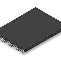
S29GL256S10TFI010 Spansion Inc., S29GL256S10TFI010 Datasheet - Page 15

S29GL256S10TFI010
Manufacturer Part Number
S29GL256S10TFI010
Description
Flash 256 MBIT 3V 100NS PAGE MODE FLASH
Manufacturer
Spansion Inc.
Datasheet
1.S29GL256S10TFI010.pdf
(97 pages)
Specifications of S29GL256S10TFI010
Data Bus Width
16 bit
Memory Type
Flash
Memory Size
256 Mbit
Architecture
Uniform
Timing Type
Asynchronous
Interface Type
CFI
Access Time
100 ns
Supply Voltage (max)
3.6 V
Supply Voltage (min)
2.7 V
Maximum Operating Current
100 mA
Operating Temperature
- 40 C to + 85 C
Mounting Style
SMD/SMT
Package / Case
TSOP-56
Lead Free Status / Rohs Status
Compliant
Available stocks
Company
Part Number
Manufacturer
Quantity
Price
Company:
Part Number:
S29GL256S10TFI010
Manufacturer:
Spansion
Quantity:
25
2.3
2.4
February 11, 2011 S29GL_128S_01GS_00_01
2.2.2
Status Register ASO
Data Polling Status ASO
Common Flash Memory Interface
The original industry format was structured to work with any memory data bus width e. g. x8, x16, x32. The ID
code values are traditionally byte wide but are located at bus width address boundaries such that
incrementing the device address inputs will read successive byte, word, or double word locations with the ID
codes always located in the least significant byte location of the data bus. Because the device data bus is
word wide each code byte is located in the lower half of each word location. The original industry format made
the high order byte always 0. Spansion has modified the format to use both bytes in some words of the
address space. For the detail description of the Device ID address map see
The JEDEC Common Flash Interface (CFI) specification (JESD68.01) defines a standardized data structure
that may be read from a flash memory device, which allows vendor-specified software algorithms to be used
for entire families of devices. The data structure contains information for system configuration such as various
electrical and timing parameters, and special functions supported by the device. Software support can then
be device-independent, Device ID-independent, and forward-and-backward-compatible for entire Flash
device families.
The system can read CFI information at the addresses within the selected sector as shown in
Common Flash Interface (ID-CFI) ASO Map on page
Like the Device ID information, CFI information is structured to work with any memory data bus width e. g. x8,
x16, x32. The code values are always byte wide but are located at data bus width address boundaries such
that incrementing the device address reads successive byte, word, or double word locations with the codes
always located in the least significant byte location of the data bus. Because the data bus is word wide each
code byte is located in the lower half of each word location and the high order byte is always 0.
For further information, please refer to the Spansion CFI Specification, Version 1.4 (or later), and the JEDEC
publications JEP137-A and JESD68.01. Please contact JEDEC (http://www.jedec.org/) for their standards
and the Spansion CFI Specification may be found at the Spansion Web site
Support/TechnicalDocuments/Pages/ApplicationNotes.aspx
contacting a local Spansion sales office listed on the web site.
The Status register ASO contains a single word of registered volatile status for Embedded Algorithms. When
the Status Register read command is issued, the current status is captured by the register and the ASO is
entered. The Status Register content appears at all word locations in the device address space. However, it is
recommended to read the status only at word location 0 for future compatibility. The first read access in the
Status Register ASO exits the ASO and returns to the address space map in use when the Status Register
read command was issued.
The Data Polling Status ASO contains a single word of volatile memory indicating the progress of an EA. The
Data Polling Status ASO is entered immediately following the last write cycle of any command sequence that
initiates an EA. Commands that initiate an EA are:
Word Program
Program Buffer to Flash
Chip Erase
Sector Erase
Erase Resume / Program Resume
Program Resume Enhanced Method
Blank Check
Lock Register Program
Password Program
PPB Program
D a t a
S h e e t
( A d v a n c e
GL-S MirrorBit
I n f o r m a t i o n )
®
Family
60.
at the time of this document's publication) or by
Table 6.2 on page
(http://www.spansion.com/
Device ID and
60.
15


