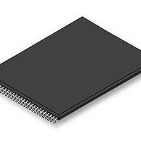
S29GL256S10TFI010 Spansion Inc., S29GL256S10TFI010 Datasheet - Page 28

S29GL256S10TFI010
Manufacturer Part Number
S29GL256S10TFI010
Description
Flash 256 MBIT 3V 100NS PAGE MODE FLASH
Manufacturer
Spansion Inc.
Datasheet
1.S29GL256S10TFI010.pdf
(97 pages)
Specifications of S29GL256S10TFI010
Data Bus Width
16 bit
Memory Type
Flash
Memory Size
256 Mbit
Architecture
Uniform
Timing Type
Asynchronous
Interface Type
CFI
Access Time
100 ns
Supply Voltage (max)
3.6 V
Supply Voltage (min)
2.7 V
Maximum Operating Current
100 mA
Operating Temperature
- 40 C to + 85 C
Mounting Style
SMD/SMT
Package / Case
TSOP-56
Lead Free Status / Rohs Status
Compliant
Available stocks
Company
Part Number
Manufacturer
Quantity
Price
Company:
Part Number:
S29GL256S10TFI010
Manufacturer:
Spansion
Quantity:
25
D a t a
S h e e t
( A d v a n c e
I n f o r m a t i o n )
Figure 5.1 Word Program Operation
START
Write Program Command
Sequence
Data Poll from System
Embedded
Program
algorithm
No
Verify Word?
in progress
Yes
No
Increment Address
Last Addresss?
Yes
Programming Completed
5.3.1.2
Write Buffer Programming
A write buffer is used to program data within a 512-byte address range aligned on a 512-byte boundary
(Line). Thus, a full Write Buffer Programming operation must be aligned on a Line boundary. Programming
operations of less than a full 512 bytes may start on any word boundary but may not cross a Line boundary.
At the start of a Write Buffer programming operation all bit locations in the buffer are all 1’s (FFFFh words)
thus any locations not loaded will retain the existing data. See
Product Overview on page 10
for information
on address map.
Write Buffer Programming allows up to 512-bytes to be programmed in one operation. It is possible to
program from 1 bit up to 512-bytes in each Write Buffer Programming operation. A 32-byte Page is the
smallest program granularity on which Automatic ECC protection is enabled. Programming the same Page
more than once will disable the Automatic ECC on that Page. It is recommended that a multiple of Pages be
written and each Page written only once. This insures that the Automatic ECC protection is enabled on each
Page. For the very best performance, programming should be done in full Lines of 512-bytes aligned on 512-
byte boundaries.
Write Buffer Programming is supported only in the main flash array or the SSR ASO.
The Write Buffer Programming operation is initiated by first writing two unlock cycles. This is followed by a
third write cycle of the Write to Buffer command with the Sector Address (SA), in which programming is to
occur. Next, the system writes the number of word locations minus 1. This tells the device how many write
buffer addresses are loaded with data and therefore when to expect the Program Buffer to flash confirm
command. The Sector Address must match in the Write to Buffer command and the Write Word Count
command. The Sector to be programmed must be unlocked (unprotected).
The system then writes the starting address / data combination. This starting address is the first address /
data pair to be programmed, and selects the write-buffer-Line address. The Sector address must match the
Write to Buffer Sector Address or the operation will abort and return to the initiating state. All subsequent
address / data pairs must be in sequential order. All write buffer addresses must be within the same Line. If
the system attempts to load data outside this range, the operation will abort and return to the initiating state.
The counter decrements for each data load operation. Note that while counting down the data writes, every
write is considered to be data being loaded into the write buffer. No commands are possible during the write
buffer loading period. The only way to stop loading the write buffer is to write with an address that is outside
the Line of the programming operation. This invalid address will immediately abort the Write to Buffer
command.
Once the specified number of write buffer locations has been loaded, the system must then write the Program
Buffer to Flash command at the Sector Address. The device then goes busy. The Embedded Program
algorithm automatically programs and verifies the data for the correct data pattern. The system is not required
to provide any controls or timings during these operations. If an incorrect number of write buffer locations
have been loaded the operation will abort and return to the initiating state. The abort occurs when anything
®
28
GL-S MirrorBit
Family
S29GL_128S_01GS_00_01 February 11, 2011


