XCARD XC-1 XMOS, XCARD XC-1 Datasheet - Page 16
XCARD XC-1
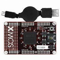
Manufacturer Part Number
XCARD XC-1
Description
BOARD DEV KIT XS1-G4
Manufacturer
XMOS
Series
XCore™r
Type
MCUr
Datasheets
1.XS1-G04B-FB144-C4.pdf
(22 pages)
2.XCARD_XC-1.pdf
(2 pages)
3.XCARD_XC-1.pdf
(21 pages)
4.XCARD_XC-1.pdf
(17 pages)
Specifications of XCARD XC-1
Contents
Board, Cable
Lead Free Status / Rohs Status
Lead free / RoHS Compliant
For Use With/related Products
XS1-G4
Other names
880-1013


XS1-G4 144BGA Datasheet (3.5)
The OTP may be programmed using its internal charge pump or by supplying a
The Input Valid window parameter relates to the capability of the XS1-G4 family
This parameter can be calculated as the sum of the input setup time and input hold
3.7.3 OTP voltage ramp requirement
6.5V VPP programming voltage on the OTP_VPP pin. Unless a programming cycle is
underway the OTP_VPP pins should be left undriven.
For further information on security and OTP programming, see the relevant applica-
tion note.
3.8 Port Timing
Ports timing is explained in a separate application note. Please see
http://xmos.com/documentation
3.8.1 XCore I/O AC Characteristics
devices to capture data input to the chip with respect to an external clock source.
time with regard to the external clock as measured at the G4 device pins. The output
invalid window specifies the time for which an output will be invalid with respect to
the external clock. Note that these parameters are specified as a window rather than
Symbol
V(PP)
Symbol
T(XOINVALID)
T(XOVALID)
T(XIFMAX)
Parameter
OTP VPP Programming Volt-
age Ramp Rate
Parameter
XCore I/O Minimum Out-
put Data Invalid window
which can be achieved
using Port/ClkBlk com-
bination
XCore I/O Minimum In-
put Data Valid window
to allow safe acquisition
of data using Port/Clk-
Blk combination
Maximum XCore I/O
toggle frequency which
can be safely acquired
and used as a clock
source using a ClkBlk
www.xmos.com
for more details.
MIN
9
8
MIN
TYP
TYP
MAX
60
MAX
1
UNITS
ns
ns
MHz
UNITS
V/ s
Notes
Notes
16/22
Related parts for XCARD XC-1
Image
Part Number
Description
Manufacturer
Datasheet
Request
R

Part Number:
Description:
BOARD DEV KIT XS1-G4 ETHERNET
Manufacturer:
XMOS
Datasheet:

Part Number:
Description:
BOARD DEV KIT XS1-G4
Manufacturer:
XMOS
Datasheet:

Part Number:
Description:
DEV KIT EVENT-DRIVEN PROC XS1-L1
Manufacturer:
XMOS
Datasheet:

Part Number:
Description:
BOARD KIT XS1-G4 LED CTRL TILE
Manufacturer:
XMOS
Datasheet:

Part Number:
Description:
ADAPTER USB DEBUGGER JTAG XSYS2
Manufacturer:
XMOS
Datasheet:

Part Number:
Description:
IC MPU 32BIT SINGLE CORE 64LQFP
Manufacturer:
XMOS
Datasheet:

Part Number:
Description:
IC MPU 32BIT SINGLE CORE 64LQFP
Manufacturer:
XMOS
Datasheet:
Part Number:
Description:
IC MPU 32BIT SINGLE CORE 64LQFP
Manufacturer:
XMOS
Datasheet:

Part Number:
Description:
IC MPU 32BIT SINGLE CORE 64LQFP
Manufacturer:
XMOS
Datasheet:
Part Number:
Description:
IC MPU 32BIT SINGLE CORE 64LQFP
Manufacturer:
XMOS
Datasheet:

Part Number:
Description:
IC MPU 32BIT SINGLE CORE 128TQFP
Manufacturer:
XMOS
Datasheet:
Part Number:
Description:
IC MPU 32BIT SINGLE CORE 64LQFP
Manufacturer:
XMOS
Datasheet:
Part Number:
Description:
IC MPU 32BIT SINGLE CORE 128TQFP
Manufacturer:
XMOS
Datasheet:
Part Number:
Description:
IC MPU 32BIT SINGLE CORE 128TQFP
Manufacturer:
XMOS
Datasheet:

Part Number:
Description:
IC MPU 32BIT DUAL CORE 124QFN
Manufacturer:
XMOS
Datasheet: