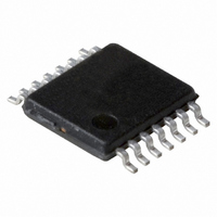
PCA9542APW/DG,118 NXP Semiconductors, PCA9542APW/DG,118 Datasheet - Page 8

PCA9542APW/DG,118
Manufacturer Part Number
PCA9542APW/DG,118
Description
IC I2C MUX 2-CH 14-TSSOP
Manufacturer
NXP Semiconductors
Datasheet
1.PCA9542APW118.pdf
(22 pages)
Specifications of PCA9542APW/DG,118
Package / Case
14-TSSOP
Applications
2-Channel I²C Multiplexer
Interface
I²C, SMBus
Voltage - Supply
2.3 V ~ 5.5 V
Mounting Type
Surface Mount
Logic Family
I2C Bus
High Level Output Current
10 uA
Low Level Output Current
3 mA
Propagation Delay Time
0.3 ns
Supply Voltage (max)
5.5 V
Supply Voltage (min)
2.3 V
Maximum Operating Temperature
+ 85 C
Minimum Operating Temperature
- 40 C
Input Signal Type
SCL / SDA
Interface Type
I2C Bus
Maximum Power Dissipation
400 mW
Mounting Style
SMD/SMT
Output Type
SCx / SDx
Lead Free Status / RoHS Status
Lead free / RoHS Compliant
Lead Free Status / RoHS Status
Lead free / RoHS Compliant, Lead free / RoHS Compliant
Other names
935286937118
PCA9542APW/DG-T
PCA9542APW/DG-T
PCA9542APW/DG-T
PCA9542APW/DG-T
NXP Semiconductors
PCA9542A_4
Product data sheet
Fig 9.
SDA
SCL
System configuration
TRANSMITTER/
RECEIVER
MASTER
7.4 Acknowledge
The number of data bytes transferred between the START and the STOP conditions from
transmitter to receiver is not limited. Each byte of eight bits is followed by one
acknowledge bit. The acknowledge bit is a HIGH level put on the bus by the transmitter,
whereas the master generates an extra acknowledge related clock pulse.
A slave receiver which is addressed must generate an acknowledge after the reception of
each byte. Also, a master must generate an acknowledge after the reception of each byte
that has been clocked out of the slave transmitter. The device that acknowledges has to
pull down the SDA line during the acknowledge clock pulse so that the SDA line is stable
LOW during the HIGH period of the acknowledge related clock pulse; set-up and hold
times must be taken into account.
A master receiver must signal an end of data to the transmitter by not generating an
acknowledge on the last byte that has been clocked out of the slave. In this event, the
transmitter must leave the data line HIGH to enable the master to generate a STOP
condition.
Fig 10. Acknowledgement on the I
RECEIVER
SLAVE
SCL from master
by transmitter
data output
by receiver
data output
TRANSMITTER/
Rev. 04 — 15 June 2009
RECEIVER
condition
START
SLAVE
S
2
C-bus
2-channel I
TRANSMITTER
1
MASTER
2
2
C-bus multiplexer and interrupt logic
TRANSMITTER/
RECEIVER
MASTER
acknowledgement
not acknowledge
SLAVE
clock pulse for
acknowledge
8
PCA9542A
MULTIPLEXER
© NXP B.V. 2009. All rights reserved.
002aaa987
I
2
9
C-BUS
002aaa966
8 of 22


