PCA9542APW/DG,118 NXP Semiconductors, PCA9542APW/DG,118 Datasheet - Page 4
PCA9542APW/DG,118
Manufacturer Part Number
PCA9542APW/DG,118
Description
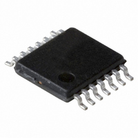
IC I2C MUX 2-CH 14-TSSOP
Manufacturer
NXP Semiconductors
Datasheet
1.PCA9542APW118.pdf
(22 pages)
Specifications of PCA9542APW/DG,118
Package / Case
14-TSSOP
Applications
2-Channel I²C Multiplexer
Interface
I²C, SMBus
Voltage - Supply
2.3 V ~ 5.5 V
Mounting Type
Surface Mount
Logic Family
I2C Bus
High Level Output Current
10 uA
Low Level Output Current
3 mA
Propagation Delay Time
0.3 ns
Supply Voltage (max)
5.5 V
Supply Voltage (min)
2.3 V
Maximum Operating Temperature
+ 85 C
Minimum Operating Temperature
- 40 C
Input Signal Type
SCL / SDA
Interface Type
I2C Bus
Maximum Power Dissipation
400 mW
Mounting Style
SMD/SMT
Output Type
SCx / SDx
Lead Free Status / RoHS Status
Lead free / RoHS Compliant
Lead Free Status / RoHS Status
Lead free / RoHS Compliant, Lead free / RoHS Compliant
Other names
935286937118
PCA9542APW/DG-T
PCA9542APW/DG-T
PCA9542APW/DG-T
PCA9542APW/DG-T


NXP Semiconductors
6. Functional description
PCA9542A_4
Product data sheet
6.2.1 Control register definition
6.1 Device addressing
6.2 Control register
Refer to
Following a START condition the bus master must output the address of the slave it is
accessing. The address of the PCA9542A is shown in
internal pull-up resistors are incorporated on the hardware selectable address pins and
they must be pulled HIGH or LOW.
The last bit of the slave address defines the operation to be performed. When set to
logic 1 a read is selected, while a logic 0 selects a write operation.
Following the successful acknowledgement of the slave address, the bus master will send
a byte to the PCA9542A which will be stored in the control register. If multiple bytes are
received by the PCA9542A, it will save the last byte received. This register can be written
and read via the I
A SCx/SDx downstream pair, or channel, is selected by the contents of the control
register. This register is written after the PCA9542A has been addressed. The 3 LSBs of
the control byte are used to determine which channel is to be selected. When a channel is
selected, it will become active after a STOP condition has been placed on the I
This ensures that all SCx/SDx lines will be in a HIGH state when the channel is made
active, so that no false conditions are generated at the time of connection.
Fig 4.
Fig 5.
Figure 1 “Block diagram of
Slave address
Control register
2
C-bus.
Rev. 04 — 15 June 2009
bit
7
X
1
6
X
1
fixed
interrupt bits
PCA9542A”.
(read only)
INT1 INT0
5
2-channel I
1
4
0
A2
X
3
selectable
hardware
enable bit
2
A1
C-bus multiplexer and interrupt logic
B2
channel selection bits
2
A0 R/W
002aab189
(read/write)
Figure
B1
1
002aae304
B0
0
4. To conserve power, no
PCA9542A
© NXP B.V. 2009. All rights reserved.
2
C-bus.
4 of 22
Related parts for PCA9542APW/DG,118
Image
Part Number
Description
Manufacturer
Datasheet
Request
R

Part Number:
Description:
IC I2C MUX 2CH 14TSSOP
Manufacturer:
NXP Semiconductors
Datasheet:
Part Number:
Description:
IC I2C MUX 2CH 14-TSSOP
Manufacturer:
NXP Semiconductors
Datasheet:

Part Number:
Description:
2-channel I2C multiplexer and interrupt controller
Manufacturer:
Philips Semiconductors
Datasheet:

Part Number:
Description:
NXP Semiconductors designed the LPC2420/2460 microcontroller around a 16-bit/32-bitARM7TDMI-S CPU core with real-time debug interfaces that include both JTAG andembedded trace
Manufacturer:
NXP Semiconductors
Datasheet:

Part Number:
Description:
NXP Semiconductors designed the LPC2458 microcontroller around a 16-bit/32-bitARM7TDMI-S CPU core with real-time debug interfaces that include both JTAG andembedded trace
Manufacturer:
NXP Semiconductors
Datasheet:
Part Number:
Description:
NXP Semiconductors designed the LPC2468 microcontroller around a 16-bit/32-bitARM7TDMI-S CPU core with real-time debug interfaces that include both JTAG andembedded trace
Manufacturer:
NXP Semiconductors
Datasheet:
Part Number:
Description:
NXP Semiconductors designed the LPC2470 microcontroller, powered by theARM7TDMI-S core, to be a highly integrated microcontroller for a wide range ofapplications that require advanced communications and high quality graphic displays
Manufacturer:
NXP Semiconductors
Datasheet:
Part Number:
Description:
NXP Semiconductors designed the LPC2478 microcontroller, powered by theARM7TDMI-S core, to be a highly integrated microcontroller for a wide range ofapplications that require advanced communications and high quality graphic displays
Manufacturer:
NXP Semiconductors
Datasheet:
Part Number:
Description:
The Philips Semiconductors XA (eXtended Architecture) family of 16-bit single-chip microcontrollers is powerful enough to easily handle the requirements of high performance embedded applications, yet inexpensive enough to compete in the market for hi
Manufacturer:
NXP Semiconductors
Datasheet:
Part Number:
Description:
The XA-S3 device is a member of Philips Semiconductors? XA(eXtended Architecture) family of high performance 16-bitsingle-chip microcontrollers
Manufacturer:
NXP Semiconductors
Datasheet:

Part Number:
Description:
The NXP BlueStreak LH75401/LH75411 family consists of two low-cost 16/32-bit System-on-Chip (SoC) devices
Manufacturer:
NXP Semiconductors
Datasheet:
Part Number:
Description:
The NXP LPC3130/3131 combine an 180 MHz ARM926EJ-S CPU core, high-speed USB2
Manufacturer:
NXP Semiconductors
Datasheet:
Part Number:
Description:
The NXP LPC3141 combine a 270 MHz ARM926EJ-S CPU core, High-speed USB 2
Manufacturer:
NXP Semiconductors
Part Number:
Description:
The NXP LPC3143 combine a 270 MHz ARM926EJ-S CPU core, High-speed USB 2
Manufacturer:
NXP Semiconductors