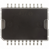
LNBS21PD-TR STMicroelectronics, LNBS21PD-TR Datasheet - Page 7

LNBS21PD-TR
Manufacturer Part Number
LNBS21PD-TR
Description
IC LNB SUPPLY & CNTRL 20-PWRSOIC
Manufacturer
STMicroelectronics
Datasheet
1.LNBS21PD-TR.pdf
(21 pages)
Specifications of LNBS21PD-TR
Applications
Power Supplies, Converters, Controllers
Interface
SMBus (2-Wire/I²C)
Voltage - Supply
8 V ~ 15 V
Package / Case
PowerSO-20 Exposed Bottom Pad
Mounting Type
Surface Mount
Output Voltage
22 V
Operating Temperature Range
- 40 C to + 125 C
Mounting Style
SMD/SMT
Lead Free Status / RoHS Status
Lead free / RoHS Compliant
Other names
497-5369-2
LNBS21PD-TR
LNBS21PD-TR
Available stocks
Company
Part Number
Manufacturer
Quantity
Price
Company:
Part Number:
LNBS21PD-TR
Manufacturer:
STM
Quantity:
690
LNBS1 SOFTWARE DESCRIPTION
INTERFACE PROTOCOL
The interface protocol comprises:
- A start condition (S)
ACK= Acknowledge
S= Start
P= Stop
R/W= Read/Write
SYSTEM REGISTER (SR, 1 BYTE)
R,W= read and write bit
R= Read-only bit
All bits reset to 0 at Power-On
TRANSMITTED DATA (I
When the R/W bit in the chip address is set to 0,
the main µP can write on the System Register
(SR) of the LNBS21 via I
X= don't care.
Values are typical unless otherwise specified
RECEIVED DATA (I
The LNBS21 can provide to the Master a copy of
the SYSTEM REGISTER information via I
in read mode. The read mode is Master activated
by sending the chip address with R/W bit set to 1.
At the following master generated clocks bits, the
LNBS21 issues a byte on the SDA data bus line
(MSB transmitted first).
At the ninth clock bit the MCU master can:
PCL
S
X
0
1
MSB
R, W
PCL
MSB
0
ISEL
X
0
1
0
TEN
X
0
1
R, W
ISEL
0
CHIP ADDRESS
2
LLC VSEL
C bus READ MODE)
X
0
0
1
1
1
2
2
C bus. Only 6 bits out of
C BUS WRITE MODE)
0
X
0
1
0
1
R, W
TEN
0
EN
1
1
1
1
1
1
1
1
1
1
0
0
OTF
X
X
X
X
X
X
X
X
X
X
X
LSB
R/W ACK
2
R, W
C bus
LLC
OLF
X
X
X
X
X
X
X
X
X
X
X
V
V
V
V
22KHz tone is controlled by DSQIN pin
22KHz tone is ON, DSQIN pin disabled
I
I
Pulsed (dynamic) current limiting is selected
Static current limiting is selected
Power blocks disabled, Loopthrough switch closed
OUT(min)
OUT(min)
MSB
OUT
OUT
OUT
OUT
- A chip address byte = hex 10 / 11 (the LSB bit
determines read(=1)/write(=0) transmission)
- A sequence of data (1 byte + acknowledge)
- A stop condition (P)
the 8 available can be written by the µP, since the
remaining 2 are left to the diagnostic flags, and are
read-only.
- acknowledge the reception, starting in this way
the transmission of another byte from the
LNBS21;
- no acknowledge, stopping the read mode
communication.
While the whole register is read back by the µP,
only the two read-only bits OLF and OTF convey
diagnostic informations about the LNBS21.
VSEL
R, W
=13V, V
=18V, V
=14V, V
=19V, V
=500mA, I
=400mA, I
UP
UP
UP
UP
=16V Loopthrough switch open
=21V Loopthrough switch open
=17V Loopthrough switch open
=22V Loopthrough switch open
OUT(max)
OUT(max)
R, W
EN
DATA
Function
=650mA I
=550mA I
OTF
R
SC
SC
=300mA
=300mA
LSB
LNBS21
ACK
LSB
OLF
R
7/21
P


