LNBS21PD-TR STMicroelectronics, LNBS21PD-TR Datasheet - Page 5
LNBS21PD-TR
Manufacturer Part Number
LNBS21PD-TR
Description
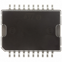
IC LNB SUPPLY & CNTRL 20-PWRSOIC
Manufacturer
STMicroelectronics
Datasheet
1.LNBS21PD-TR.pdf
(21 pages)
Specifications of LNBS21PD-TR
Applications
Power Supplies, Converters, Controllers
Interface
SMBus (2-Wire/I²C)
Voltage - Supply
8 V ~ 15 V
Package / Case
PowerSO-20 Exposed Bottom Pad
Mounting Type
Surface Mount
Output Voltage
22 V
Operating Temperature Range
- 40 C to + 125 C
Mounting Style
SMD/SMT
Lead Free Status / RoHS Status
Lead free / RoHS Compliant
Other names
497-5369-2
LNBS21PD-TR
LNBS21PD-TR
Available stocks
Company
Part Number
Manufacturer
Quantity
Price
Company:

Part Number:
LNBS21PD-TR
Manufacturer:
STM
Quantity:
690


Figure 3: Typical Application Circuit
(*) Set to GND if not used
(**) filter to be used according to EUTELSAT recommendation to implement the DiSEqC
not implemented (see DiSEqC implementation note)
(***) IC2 is a ST Fettky, STS4DNFS30L, that includes both the schottky diode and the N-Channel MosFet, needed for the DC/DC converter,
in a So-8 package. It can be replaced by a schottky diode (STPS2L3A or similar) and a N-Channel MosFet (STN4NF03L or similar)
I
Data transmission from main µP to the LNBS21
and viceversa takes place through the 2 wires I
bus interface, consisting of the two lines SDA and
SCL (pull-up resistors to positive supply voltage
must be externally connected).
DATA VALIDITY
As shown in fig. 1, the data on the SDA line must
be stable during the high period of the clock. The
HIGH and LOW state of the data line can only
change when the clock signal on the SCL line is
LOW.
START AND STOP CONDITIONS
As shown in fig.2 a start condition is a HIGH to
LOW transition of the SDA line while SCL is HIGH.
The stop condition is a LOW to HIGH transition of
the SDA line while SCL is HIGH. A STOP
conditions must be sent before each START
condition.
BYTE FORMAT
2
C BUS INTERFACE
(Note 3)
IC2
L1=22µH
12V
Vin
STS4DNFS30L
R
0.1
sc
C1
220µF
C2
220µF
(Note 4)
C4
470nF
Ceramic
C3
470nF
Ceramic
IC1
DSQIN(Note 1)
Vup
Gate
Sense
Vcc
SCL
SDA
2
C
LNBS21
D1 1N4001
GND
Every byte transferred to the SDA line must
contain 8 bits. Each byte must be followed by an
acknowledge bit. The MSB is transferred first.
ACKNOWLEDGE
The master (µP) puts a resistive HIGH level on the
SDA line during the acknowledge clock pulse (see
fig.
acknowledges has to pull-down (LOW) the SDA
line during the acknowledge clock pulse, so that
the SDA line is stable LOW during this clock pulse.
The peripheral which has been addressed has to
generate an acknowledge after the reception of
each byte, otherwise the SDA line remains at the
HIGH level during the ninth clock pulse time. In
this case the master transmitter can generate the
STOP information in order to abort the transfer.
The LNBS21 won't generate the acknowledge if
the V
threshold (6.7V typ.).
TRANSMISSION WITHOUT ACKNOWLEDGE
Avoiding to detect the acknowledge of the
LNBS21, the µP can use a simpler transmission:
ADDRESS
CC
DSQOUT
3).
DETIN
(Note 1)
EXTM
supply is below the Undervoltage Lockout
Byp
LT1
LT2
Vo
TM
The
2.x, not needed if bidirectional DiSEqC
C8
10nF
peripheral
C5
470nF
C6
10nF
D2
BAT43
C7
10nF
0<Vaddr<V
Master STB
see Note 2
15 ohm
270µH
Byp
(LNBS21)
to LNB
LNBS21
TM
2.x is
5/21
that
Related parts for LNBS21PD-TR
Image
Part Number
Description
Manufacturer
Datasheet
Request
R

Part Number:
Description:
Lnb Supply And Control Ic With Step-up Converter And I2c Interface
Manufacturer:
STMicroelectronics
Datasheet:
Part Number:
Description:
LNBs supply and control IC with step-up and I2C interface
Manufacturer:
STMicroelectronics
Datasheet:
Part Number:
Description:
Lnbs Supply And Control Ic With Step-up And I??c Interface
Manufacturer:
STMicroelectronics
Datasheet:
Part Number:
Description:
STMicroelectronics [RIPPLE-CARRY BINARY COUNTER/DIVIDERS]
Manufacturer:
STMicroelectronics
Datasheet:
Part Number:
Description:
STMicroelectronics [LIQUID-CRYSTAL DISPLAY DRIVERS]
Manufacturer:
STMicroelectronics
Datasheet:

Part Number:
Description:
BOARD EVAL FOR MEMS SENSORS
Manufacturer:
STMicroelectronics
Datasheet:
Part Number:
Description:
NPN TRANSISTOR POWER MODULE
Manufacturer:
STMicroelectronics
Datasheet:
Part Number:
Description:
TURBOSWITCH ULTRA-FAST HIGH VOLTAGE DIODE
Manufacturer:
STMicroelectronics
Datasheet:
Part Number:
Description:
Manufacturer:
STMicroelectronics
Datasheet:
Part Number:
Description:
DIODE / SCR MODULE
Manufacturer:
STMicroelectronics
Datasheet:
Part Number:
Description:
DIODE / SCR MODULE
Manufacturer:
STMicroelectronics
Datasheet:
Part Number:
Description:
Search -----> STE16N100
Manufacturer:
STMicroelectronics
Datasheet: