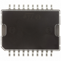
LNBS21PD-TR STMicroelectronics, LNBS21PD-TR Datasheet

LNBS21PD-TR
Specifications of LNBS21PD-TR
LNBS21PD-TR
Available stocks
Related parts for LNBS21PD-TR
LNBS21PD-TR Summary of contents
Page 1
STEP-UP CONVERTER AND I COMPLETE INTERFACE BETWEEN LNB 2 TM AND I C BUS BUILT-IN DC/DC CONTROLLER FOR SINGLE 12V SUPPLY OPERATION ACCURATE BUILT-IN 22KHz TONE OSCILLATOR SUITS WIDELY ACCEPTED STANDARDS FAST OSCILLATOR START-UP FACILITATES TM DiSEqC ENCODING BUILT-IN 22KHz ...
Page 2
LNBS21 post-regulator to work at a minimum dissipated power. An UnderVoltage Lockout circuit will disable the whole circuit when the supplied V drops below a fixed threshold (6.7V typically). The internal 22KHz tone generator is factory trimmed in accordance to ...
Page 3
... Absolute Maximum Ratings are those values beyond which damage to the device may occur. Functional operation under these condition is not implied. Table 3: Thermal Data Symbol R Thermal Resistance Junction-case thj-case Figure 2: Pin Connection (top view) PowerSO-20 (Tube) LNBS21PD Parameter Parameter PowerSO-20 LNBS21 PowerSO-20 (Tape & Reel) LNBS21PD-TR Value Unit Internally Limited ...
Page 4
LNBS21 Table 4: Pin Description SYMBOL NAME V Supply Input CC GATE External Switch Gate SENSE Current Sense Input V Step-up Voltage up OUT Output Port SDA Serial Data SCL Serial Clock DSQIN DiSEqC Input DETIN Detector In DSQOUT DiSEqC ...
Page 5
Figure 3: Typical Application Circuit C2 220µF IC2 STS4DNFS30L (Note 3) L1=22µ (Note 4) 0.1 C1 220µF Vin 12V (*) Set to GND if not used (**) filter to be used according to EUTELSAT recommendation to implement the ...
Page 6
LNBS21 simply it waits one clock without checking the slave acknowledging, and sends the new data. Figure 4: Data Validity On The I Figure 5: Timing Diagram Figure 6: Acknowledge On I 6/21 This approach of course ...
Page 7
LNBS1 SOFTWARE DESCRIPTION INTERFACE PROTOCOL The interface protocol comprises start condition (S) CHIP ADDRESS MSB ACK= Acknowledge S= Start P= Stop R/W= Read/Write SYSTEM REGISTER (SR, 1 BYTE) MSB ...
Page 8
LNBS21 PCL ISEL TEN LLC VSEL These bits are read exactly the same as they were left after last write operation Values are typical unless otherwise specified 2 POWER- INTERFACE RESET 2 The I C interface built in ...
Page 9
Symbol Parameter V Line Regulation O V Load Regulation O I Output Current Limiting MAX I Output Short Circuit Current SC t Dynamic Overload OFF protection OFF Time t Dynamic Overload ON protection ON Time f Tone Frequency TONE A ...
Page 10
LNBS21 Table 6: Gate And Sense Electrical Characteristics (T Symbol Parameter R Gate LOW R DSON-L DSON R Gate LOW R DSON-H DSON V Current Limit Sense Voltage SENSE 2 Table Electrical Characteristics (T Symbol Parameter V ...
Page 11
TYPICAL CHARACTERISTICS (unless otherwise specified T Figure 8: Output Voltage vs Temperature Figure 9: Output Voltage vs Temperature Figure 10: Line Regulation vs Temperature = 25°C) j Figure 11: Line Regulation vs Temperature Figure 12: Load Regulation vs Temperature Figure ...
Page 12
LNBS21 Figure 14: Supply Current vs Temperature Figure 15: Supply Current vs Temperature Figure 16: Dynamic Overload Protection ON Time vs Temperature 12/21 Figure 17: Dynamic Overload Protection OFF Time vs Temperature Figure 18: Output Current Limiting vs Temperature Figure ...
Page 13
Figure 20: Tone Frequency vs Temperature Figure 21: Tone Amplitude vs Temperature Figure 22: Tone Duty Cycle vs Temperature Figure 23: Tone Rise Time vs Temperature Figure 24: Tone Fall Time vs Temperature Figure 25: Loopthrought Switch Drop Voltage vs ...
Page 14
LNBS21 Figure 26: Loopthrought Switch Drop Voltage vs Temperature Figure 27: Loopthrought Switch Drop Voltage vs Loopthrought Current Figure 28: Loopthrought Switch Drop Voltage vs Loopthrought Current 14/21 Figure 29: DSQOUT Pin Logic Low vs Temperature Figure 30: Undervoltage Lockout ...
Page 15
Figure 32: DC/DC Converter Efficiency vs Temperature Figure 33: Current Limit Sense vs Temperature Figure 34: 22kHz Tone V =12V, I =50mA, EN=TEN Figure 35: DSQIN Tone Enable Transient Response V =12V, I =50mA, EN=1, TEN ...
Page 16
LNBS21 Figure 38: Output Voltage Transient Response from 13V to 18V V =12V, I =50mA, VSEL=from EN TERMAL DESIGN NOTES During normal operation, this device dissipates some power. At maximum rated output current (500mA), the ...
Page 17
Figure 40: SO-20 Suggested Pcb Heatsink Layout Figure 41: PowerSO-20 Suggested Pcb Heatsink Layout LNBS21 17/21 ...
Page 18
LNBS21 DIM. MIN 0. 0.40 c 0.23 D (1) 15.80 E 13. (1) 10. 0. 0˚ T (1) “D and E1” do not include ...
Page 19
Tape & Reel PowerSO-20 MECHANICAL DATA mm. DIM. MIN. TYP A C 12 15.1 Bo 16.5 Ko 3.8 Po 3.9 P 23.9 W 23.7 MAX. MIN. 330 13.2 0.504 0.795 2.362 30.4 15.3 0.594 ...
Page 20
LNBS21 Table 9: Revision History Date Revision 05-Oct-2004 3 20/21 Description of Changes Mistake Pin 6 - Table 4. ...
Page 21
... No license is granted by implication or otherwise under any patent or patent rights of STMicroelectronics. Specifications mentioned in this publication are subject to change without notice. This publication supersedes and replaces all information previously supplied. STMicroelectronics products are not authorized for use as critical components in life support devices or systems without express written approval of STMicroelectronics ...


