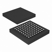
PX1011B-EL1/G,551 NXP Semiconductors, PX1011B-EL1/G,551 Datasheet - Page 10

PX1011B-EL1/G,551
Manufacturer Part Number
PX1011B-EL1/G,551
Description
IC PCI-EXPRESS X1 PHY 81-LFBGA
Manufacturer
NXP Semiconductors
Specifications of PX1011B-EL1/G,551
Package / Case
81-LFBGA
Applications
PCI Express MAX to PCI Express PHY
Interface
JTAG
Voltage - Supply
1.2 V
Mounting Type
Surface Mount
Input Voltage Range (max)
0.31 V
Maximum Operating Temperature
+ 70 C
Maximum Power Dissipation
300 mW
Minimum Operating Temperature
0 C
Mounting Style
SMD/SMT
Operating Supply Voltage
1.2 V
Supply Current (max)
28 mA
Lead Free Status / RoHS Status
Lead free / RoHS Compliant
Lead Free Status / RoHS Status
Lead free / RoHS Compliant, Lead free / RoHS Compliant
Other names
568-4715
935282113551
PX1011B-EL1/G-S
PX1011B-EL1/G-S
935282113551
PX1011B-EL1/G-S
PX1011B-EL1/G-S
Available stocks
Company
Part Number
Manufacturer
Quantity
Price
Company:
Part Number:
PX1011B-EL1/G,551
Manufacturer:
NXP Semiconductors
Quantity:
10 000
NXP Semiconductors
PX1011B_4
Product data sheet
8.5 Power management
The power management signals allow the PHY to manage power consumption. The PHY
meets all timing constraints provided in the PCI Express base specification regarding
clock recovery and link training for the various power states.
Four power states are defined: P0, P0s, P1 and P2. P0 state is the normal operational
state for the PHY. When directed from P0 to a lower power state, the PHY can
immediately take whatever power saving measures are appropriate.
In states P0, P0s and P1, the PHY keeps internal clocks operational. For all state
transitions between these three states, the PHY indicates successful transition into the
designated power state by a single cycle assertion of PHYSTATUS. For all power state
transitions, the MAC must not begin any operational sequences or further power state
transitions until the PHY has indicated that the initial state transition is completed. TXIDLE
should be asserted while in power states P0s and P1.
While the PHY is in either P0 or P0s power states, if the receiver is detecting an electrical
idle, the receiver portion of the PHY can take appropriate power saving measures. Note
that the PHY is capable of obtaining bit and symbol lock within the PHY-specified time
(N_FTS with or without common clock) upon resumption of signaling on the receive
channel. This requirement only applies if the receiver had previously been bit and symbol
locked while in P0 or P0s states.
Fig 4.
•
•
•
•
PHYSTATUS
P0 state: All internal clocks in the PHY are operational. P0 is the only state where the
PHY transmits and receives PCI Express signaling. P0 is the appropriate PHY power
management state for most states in the Link Training and Status State Machine
(LTSSM). Exceptions are listed for each lower power PHY state (P0s, P1 and P2).
P0s state: The MAC will move the PHY to this state only when the transmit channel is
idle.
P1 state: Selected internal clocks in the PHY are turned off. The MAC will move the
PHY to this state only when both transmit and receive channels are idle. The PHY
indicates a successful entry into P1 (by asserting PHYSTATUS). P1 should be used
for the disabled state, all detect states, and L1.idle state of the Link Training and
Status State Machine (LTSSM).
P2 state: PHY will enter P1 instead.
RESET_N
RXCLK
Reset
Rev. 04 — 4 September 2009
100 MHz
PCI Express stand-alone X1 PHY
250 MHz
PX1011B
© NXP B.V. 2009. All rights reserved.
002aac172
10 of 30


